[CMSC 411 Home] | [Syllabus] | [Project] | [VHDL resource] | [Homework 1-6] | [Homework 7-12] [Files] |
The goal of the semester project is to design and simulate a pipelined RISC CPU. Major components will be the pipelined ALU data path, the instruction decoder, hazard detection and associated forwarding/stall and cache memory controller.
You will get a  -0  or worse, on any project part that is
a copy of a previous semesters project. DO NOT COPY !
 The project is to be submitted on GL as five transactions for five files:
   submit cs411 part1 part1.vhdl
   submit cs411 part2 part2a.vhdl
   submit cs411 part2 part2b.vhdl
   submit cs411 part3 part3a.vhdl
   submit cs411 part3 part3b.vhdl

 The files you submit are not the starter files but the starter files
 with your additions to make it work.
  IF you have not already done this for HW4 and HW6:

  First: You must ssh to cadence.gl.umbc.edu because the Cadence
         software is licensed to this machine.

  Next: Follow instructions exactly or you figure out a variation.
        be in your home directory on cadence1 or 2 and then type commands:

      cp /afs/umbc.edu/users/s/q/squire/pub/cs411.tar  .
      tar -xvf cs411.tar
      cd vhdl
      tcsh
      source vhdl_cshrc
      make
      more add32_test.out
      make clean              # saves a lot of disk quota

    Then do your own thing with Makefile for parts of the project
    You can most easily use this directory for HW4, HW6, and
    the five parts of the project.
 Starter files may be copied to your vhdl subdirectory on
 cadence1.cs.umbc.edu  using commands such as:

 cp  /afs/umbc.edu/users/s/q/squire/pub/part1_start.vhdl .
 cp  /afs/umbc.edu/users/s/q/squire/pub/cs411_opcodes.txt .
 cp  /afs/umbc.edu/users/s/q/squire/pub/bshift.vhdl .
 cp  /afs/umbc.edu/users/s/q/squire/pub/part1.abs .
 cp  /afs/umbc.edu/users/s/q/squire/pub/part1.run .
 cp  /afs/umbc.edu/users/s/q/squire/pub/part1.chk .
 cp  /afs/umbc.edu/users/s/q/squire/pub/part1.ps  .
 cp  /afs/umbc.edu/users/s/q/squire/pub/alu.ps  .

 For Symphoney EDA VHDL
 cp  /afs/umbc.edu/users/s/q/squire/pub/part1.chks .
 cp  /afs/umbc.edu/users/s/q/squire/pub/make.bat  . # Windows
PART1: Handle lw, sw, add, sub, and, addi, sll, srl, cmpl and nop
with no hazards.
(nop's are inserted in the part1.abs file to prevent hazards.)
See cs411_opcodes.txt for detailed instruction formats and definitions.
See reglist.txt for register use conventions.
You should use part1_start.vhdl as a start for coding your circuit.
You can do your own shift circuit or use the bshift.vhdl component.
Quick start steps:
1) copy part1_start.vhdl to part1.vhdl then work on project in part1.vhdl
2) replace all "part1_start" with "part1"
3) fill in VHDL for the ALU_32 architecture to implement
sub, and, sll, srl, cmpl. All other instructions must do a plain add.
Note that EX_IR coming into ALU_32 has the instruction in "inst"
and a possible schematic is alu.jpg and alu.ps
Hints on coding the ALU.
4) compute the signals RegDst
ALUSrc
MEMWrite
WB_write_enb (needs 'or' of more opcodes)
Use MEM_lw:entity WORK.equal6(...)
as an example for setting a mux control based on opcode.
In each stage **_IR is the instruction currently in that stage.
**_IR(31 downto 26) is the six bit major op code. "100011" for lw
**_IR(5 downto 0) is the six bit minor op code. "100000" for add.
5) Compile, analyze, run using commands in your Makefile
part1.out: part1.vhdl add32.vhdl bshift.vhdl part1.run part1.abs
ncvhdl -v93 add32.vhdl
ncvhdl -v93 bshift.vhdl
ncvhdl -v93 part1.vhdl # renamed and modified part1_start.vhdl
ncelab -v93 part1:schematic
ncsim -batch -logfile part1.out -input part1.run part1
diff -w part1.out part1.chk should be no differences
no stalls, timing should be exact
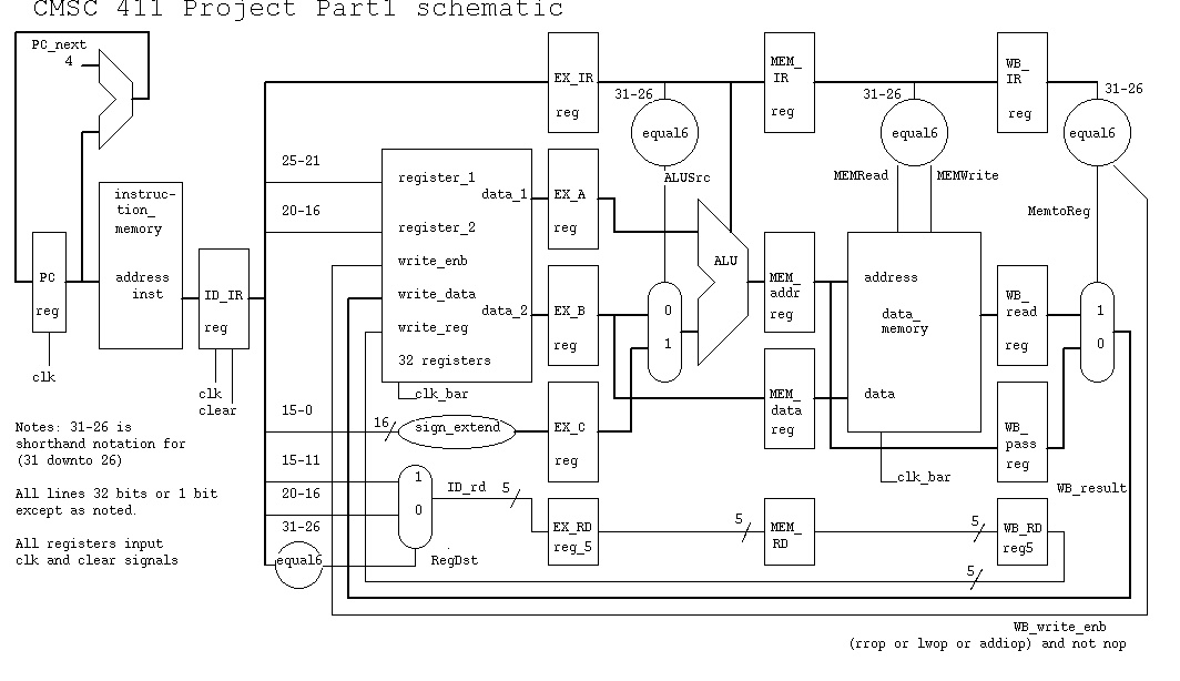
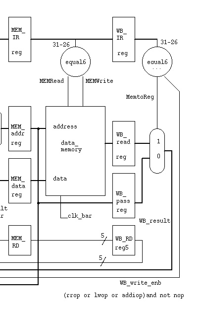
The CS411 Project Part 1 uses a modified book Figure 6.12
as shown in part1.jpg and part1.ps
For grading reasons, keep the signal names that
are pipeline registers and the entity/memory names.
The resulting output should be as shown in
part1.chk file based on part1.abs and part1.run .
Check the results in part1.out to be sure the instructions
worked. You can follow each instruction through the pipeline
by following the instruction register, *_IR and check the
*_* signals for correct values at each stage.
It is possible that your part1.out does not agree with
part1.chk but you should
be able to explain why. (Probably different don't care choices.)
You may want to copy part1.vhdl to another file and add more
'write' statements to print out more internal signal names in order
to help debug your circuit. debug.txt
Submit all components and your main circuit as one plain text
file using submit. No makefiles or run files or output is to be
submitted. Partial credit will be given based on number of
instructions simulated correctly. The starter file part1_start.vhdl
only simulates the lw instruction correctly.
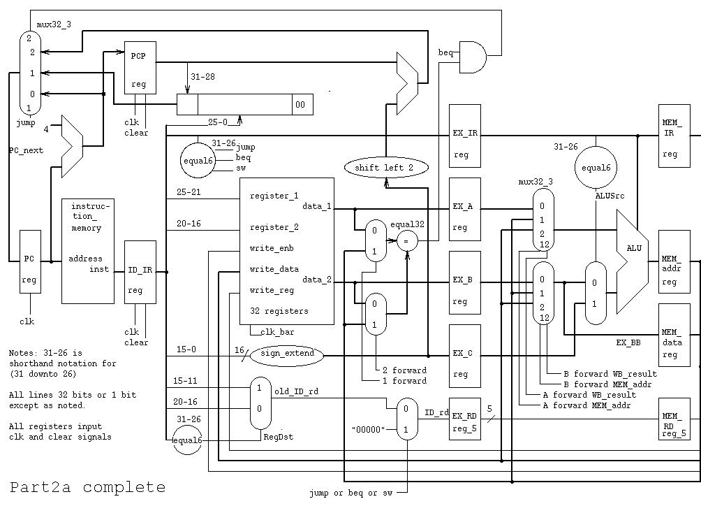
PART2: Copy your part1.vhdl to part2a.vhdl
Substitute string "part2a" for every "part1"
implement data forwarding and jump and branch.
CS411 does the branch and jump in the ID stage
CS411 goes beyond the book by forwarding for beq.
submit cs411 part2 part2a.vhdl # before working part2b
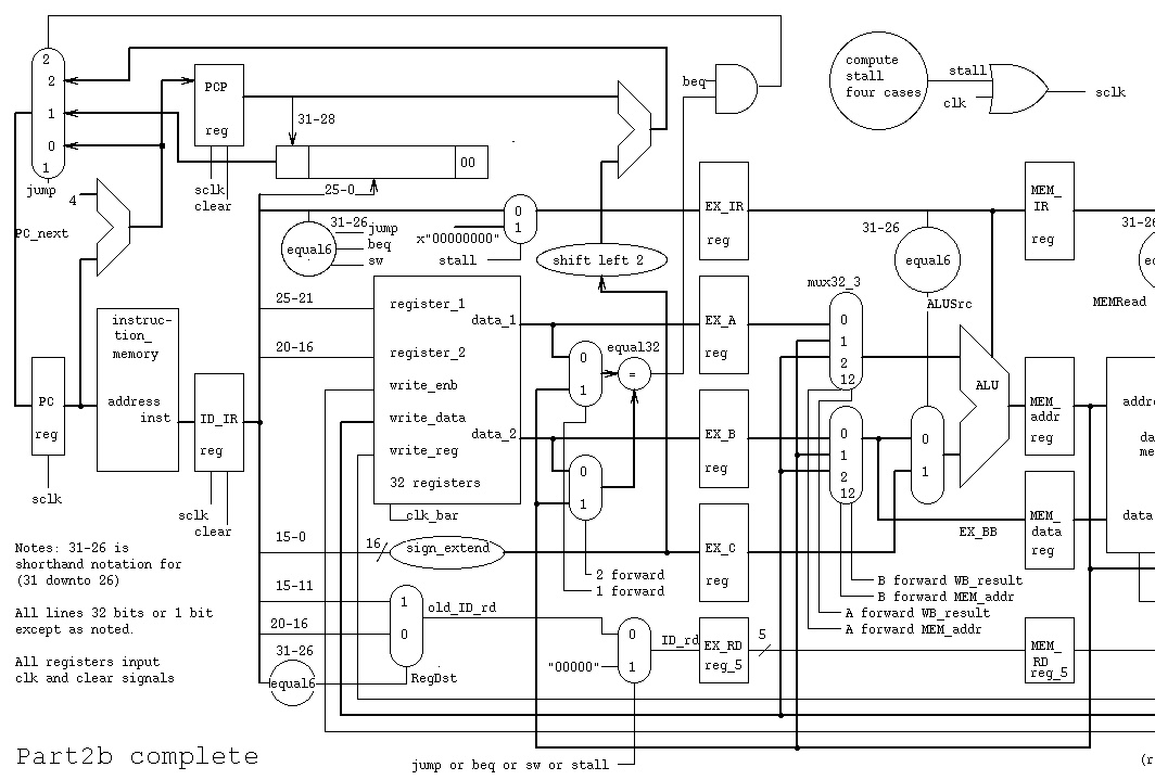
Copy your part2a.vhdl to part2b.vhdl
Substitute string "part2b" for every "part2a"
implement hazard detection and stall the minimum possible.
Data forwarding paths must cover at least those in Fig 6.51, p499.
Additional insight may be gained from a comparison of the
pipeline stages with and without data forwarding in forward.txt
A possible implementation of forwarding is forward_mem.jpg
The EX stage forwarding may use entity mux_32_3,
a multiplexor with three 32-bit inputs.
Note: jump and beq are followed by a delayed branch slot that
contains an instruction that is always executed. jump can not
cause a stall. If beq does not get data forwarding, then it
can stall, and stall, and stall. Add data forwarding for beq
by adding two mux's in the ID STAGE that get inputs from the
MEM stage as shown in part2a.jpg
or part2a.ps
Handle hazards. Detect hazards, prevent wrong results by
stalling when necessary. A stall is implemented by holding
the instruction in the ID stage and letting the EX, MEM and
WB stages proceed. The stall signal prevents the IF and ID
stages from getting a clock signal. A terse summary of the
hazard detection is in hazard.txt
A possible implementation of hazards is stall_lw.jpg
The CS411 Project Part 2b uses a modified book Figure 6.65
as shown in part2b.jpg and part2b.ps
Implement your circuit assuming that software has correctly
filled the delayed branch slot and implement the branch in
the ID stage as modified for this class project.
You may use the mux32_3
For grading reasons, keep the signal names that
are pipeline registers and the component/memory names.
Download files part2a.abs and part2a.run and part2a.chk
Run the following commands to check your work.
ncvhdl -v93 add32.vhdl
ncvhdl -v93 bshift.vhdl
ncvhdl -v93 part2a.vhdl # renamed and modified part1.vhdl
ncelab -v93 part2a:schematic
ncsim -batch -logfile part2a.out -input part2a.run part2a
diff -w part2a.out part2a.chk
Download files part2b.abs and part2b.run and part2b.chk
Run the following commands to check your work.
ncvhdl -v93 add32.vhdl
ncvhdl -v93 bshift.vhdl
ncvhdl -v93 part2b.vhdl # renamed and modified part2a.vhdl
ncelab -v93 part2b:schematic
ncsim -batch -logfile part2b.out -input part2b.run part2b
diff -w part2b.out part2b.chk
Part2a needs only data forwarding, jump and branch
there is no need for stalls.
Part2b needs both data forwarding and hazards (stalls)
Submit all components and your main circuit as one plain text
file using 'submit'. No makefiles or run files or output is to be
submitted. Partial credit will be given based on number of
data forwards, jump, beq, and hazard stalls handled correctly.
Your circuit will not be tested with jump or branch or data
addresses greater than 10 bits, in other words your instruction
and data memories do not need to be bigger than 1024 words.
You may not get exactly the .chk results.
Timing and stalls will be graded. Points will
be deducted for memory or register differences
or improper stalls.
PART3: Copy your part2b.vhdl to part3a.vhdl
Substitute "part3a" for every "part2b"
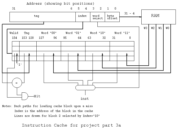
Implement a cache in the instruction memory (read only)
submit cs411 part3 part3a.vhdl
Copy your part3a.vhdl to part3b.vhdl
Substitute "part3b" for every "part3a"
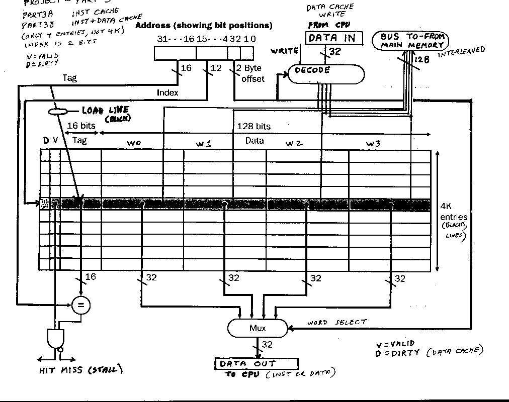
Implement a cache in the data memory (read/write)
submit cs411 part3 part3b.vhdl
Put the caches inside the instruction memory and
and data memory components (entity and architecture).
(you will need to pass a few extra signals in and out)
Use the existing shared memory data as the main memory.
Make a miss on the instruction cache cause a three cycle stall.
Make a miss on the data cache cause a four cycle stall.
Previous stalls from part2b must still work.
Both instruction cache and data cache hold 16 words
organized as four blocks of four words. Remember vhdl
memory is addressed by word address, the MIPS/SGI memory
is addressed by byte address and a cache is addressed by
block number.
Fig 7.10, page 557 is a possible read only cache for
the instruction memory. Another view of the Icache is icache.jpg
Possible, not required, VHDL to set up the start of a cache:
(no partial credit for just putting this in your cache.)
-- add in or out signals to entity instruction_memory as needed
-- for example, 'clk' 'clear' 'miss'
architecture behavior of instruction_memory is
subtype block_type is std_logic_vector(154 downto 0);
type cache_type is array (0 to 3) of block_type;
signal cache : cache_type := (others=>(others=>'0'));
-- now we have a cache memory initialized to zero
begin -- behavior
inst_mem:
process ... -- whatever, does not have to be just 'addr'
variable quad_word_addr : natural; -- for memory fetch
variable cblock : block_type;-- the shaded block in the cache
variable index : natural; -- index into cache to get a block
variable word : natural; -- select a word
variable my_line : line; -- for debug printout
...
begin
...
index := to_integer(addr(5 downto 4));
word := to_integer(addr(3 downto 2));
cblock := cache(index); -- has valid (154), tag (153 downto 128)
-- W0 (127 downto 96), W1(95 downto 64)
-- W2(63 downto 32), W3 (31 downto 0)
-- cblock is the shaded block in Fig 7.10
...
quad_word_address := to_integer(addr(13 downto 4));
W0 := memory(quad_word_address*4+0);
W1 := memory(quad_word_address*4+1); -- ...
-- fill in cblock with new words, then
cache(index) <= cblock after 30 ns; -- 3 clock delay
miss <= '1', '0' after 30 ns; -- miss is '1' for 30 ns
...
-- the part3a.chk file has 'inst' set to zero while 'miss' is 1
-- not required but cleans up the "diff"
For debugging your cache, you might find it convenient to add
this 'debug' print process inside the instruction_memory architecture:
Then diff -w part3a.out part3a_print.chk
debug: process -- used to print contents of I cache
variable my_line : LINE; -- not part of working circuit
begin
wait for 9.5 ns; -- just before rising clock
for I in 0 to 3 loop
write(my_line, string'("line="));
write(my_line, I);
write(my_line, string'(" V="));
write(my_line, cache(I)(154));
write(my_line, string'(" tag="));
hwrite(my_line, cache(I)(151 downto 128)); -- ignore top bits
write(my_line, string'(" w0="));
hwrite(my_line, cache(I)(127 downto 96));
write(my_line, string'(" w1="));
hwrite(my_line, cache(I)(95 downto 64));
write(my_line, string'(" w2="));
hwrite(my_line, cache(I)(63 downto 32));
write(my_line, string'(" w3="));
hwrite(my_line, cache(I)(31 downto 0));
writeline(output, my_line);
end loop;
wait for 0.5 ns; -- rest of clock
end process debug;
see part3a_print.chk with debug
You submit on GL using: submit cs411 part3 part3a.vhdl
Do a write through cache for the data memory.
(It must work to the point that results in main memory are
correct at the end of the run and the timing is correct,
partial credit for partial functionality)
You submit this as part3b.vhdl
The CS411 Project Part 3 uses a modified book Figure 7.10
as shown in part3.gif
For grading reasons, keep the signal names that
are pipeline registers and the component/memory names.
Test first with only instruction cache.
Download files part3a.abs and part3a.run and part3a.chk
Run the following commands to check your work.
ncvhdl -v93 add32.vhdl
ncvhdl -v93 bshift.vhdl
ncvhdl -v93 part3a.vhdl # renamed and modified part2b.vhdl
ncelab -v93 part3a:schematic
ncsim -batch -logfile part3a.out -input part3a.run part3a
diff -w part3a.out part3a.chk
Test with part3a.run and part3a.chk
Submit instruction cache only as part3a.vhdl
Test with both instruction and data cache.
Download files part3b.abs and part3b.run and part3b.chk
Run the following commands to check your work.
ncvhdl -v93 add32.vhdl
ncvhdl -v93 bshift.vhdl
ncvhdl -v93 part3b.vhdl # renamed and modified part3a.vhdl
ncelab -v93 part3b:schematic
ncsim -batch -logfile part3b.out -input part3b.run part3b
diff -w part3b.out part3b.chk
Test with part3b.run and part3b.chk or part3b_print.chk
Submit instruction cache and data cache combined as part3b.vhdl
Submit all components and your main circuit as one plain text
file by using 'submit'. No makefiles or run files or output is to be
submitted. Partial credit will be given based on number of
instructions simulated correctly, number of hazards handled
correctly and proper operation of Icache and Dcache.
Last updated 12/5/03