|
|
| PJRC.COM Offline Archive, February 07, 2004 Visit this page on the live site |
| ||
|
Shopping Cart
|
| Home | MP3 Player | 8051 Tools | All Projects | PJRC Store | Site Map |
|
You are here:
MP3 Player
| Search PJRC |
Student Project Alert: Many students request this schematic. Many student projects have a scope of work where using this design is legitimate, like this student project where they tried to write ATAPI drivers. For student projects which mandate original hardware design work (not just construction or modification of an existing design), using this large and complex design would be very unwise, as it is more sophisticated than a typical student project. The older design is realistic for a student project. It wouldn't be hard to convert that design to the STA013/CS4334, using the How To Use The STA013 page (that also includes working code).
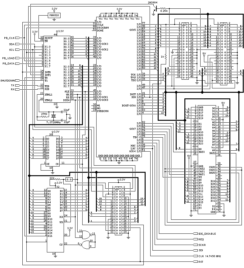
Figure 1: Processor Section |
The schematics on this page describe all of the wiring on the circuit board. Inside inside of the FPGA is described on a separate FPGA schematic page. The circuitry implemented inside the FPGA is configured by the firmware when the board boots, so that circuitry may be changed with the firmware upgrades.
The SDA and SCL lines are mis-labeled in figure 1. P1.0 is the SCL signal, and P1.1 is SDA.
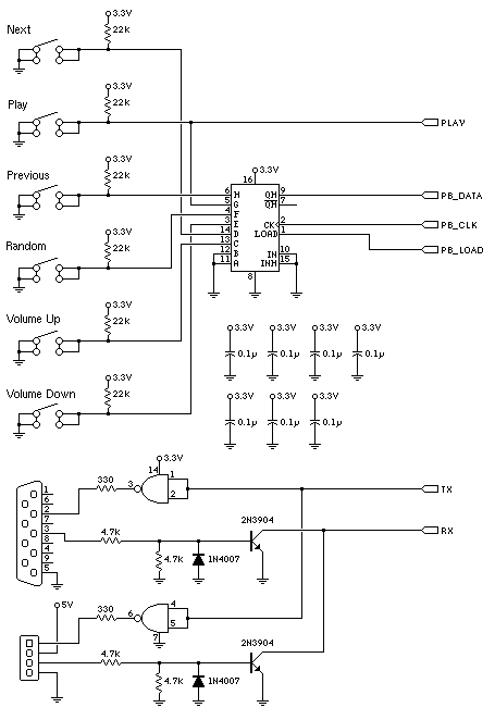
Figure 2: Interface Section |
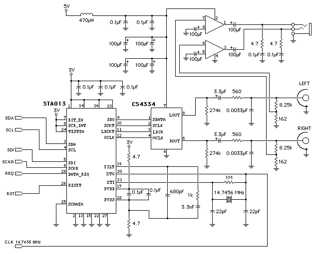
Figure 3: MP3 Decoder and Audio Section |
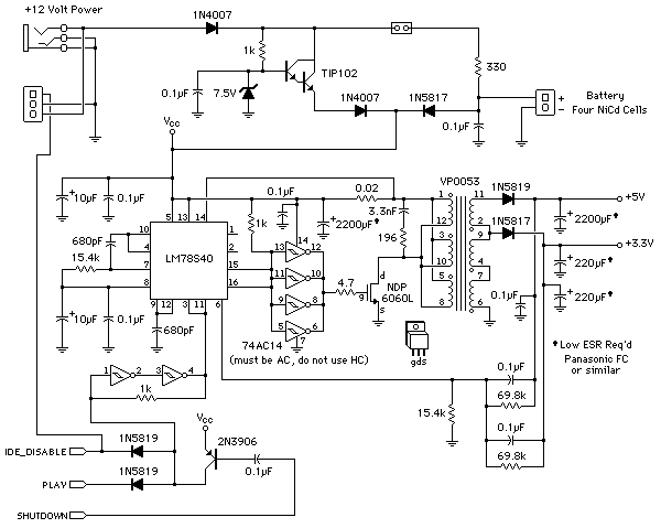
Figure 4: Power Supply Section |