<- previous index next ->
The CPU can be described by control paths and data paths.
We will look at a much simpler architecture than the Intel.
The pipeline for this architecture has stages.
All registers in each stage use the system clk
with exception of writing into a register uses clk_bar.
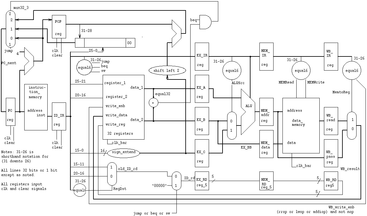 Follow an instruction through the piplined architecture.
a few opcodes
The branch slot, programming to avoid delays (filling in nop's):
Note: beq and jump always execute the next physical instruction.
This is called the "delayed branch slot".
if(a==b) x=3; /* simple C code */
else x=4;
y=5;
lw $1,a # possible unoptimized assembly language
lw $2,b # no ($0) shown on memory access
nop # wait for b to get into register 2
nop # wait for b to get into register 2
beq $1,$2,lab1
nop # branch slot, always executed *********
lwim $1,4 # else part
nop # wait for 4 to get into register 1
nop # wait for 4 to get into register 1
sw $1,x # x=4;
j lab2
nop # branch slot, always executed *********
lab1: lwim $1,3 # true part
nop # wait for 3 to get into register 1
nop # wait for 3 to get into register 1
sw $1,x # x=3;
lab2: lwim $1,5 # after if-else, always execute
nop # wait for 5 to get into register 1
nop # wait for 5 to get into register 1
sw $1,y # y=5;
Unoptimized, 20 instructions.
Now, a smart compiler would produce the optimized code:
lw $1,a # possible unoptimized assembly language
lw $2,b # no ($0) shown on memory access
lwim $4,4 # for else part later
lwim $3,3 # for true part later
beq $1,$2,lab1
lwim $5,5 # branch slot, always executed, for after if-else
j lab2
sw $4,x # x=4; in branch slot, always executed !! after jump
lab1: sw $3,x # x=3;
lab2: sw $5,y # y=5;
Optimized, 10 instructions.
The pipeline stage diagram for a==b true is:
1 2 3 4 5 6 7 8 9 10 11 12 clock
lw $1,a IF ID EX MM WB
lw $2,b IF ID EX MM WB
lwim $4,4 IF ID EX MM WB
lwim $3,3 IF ID EX MM WB
beq $1,$2,L1 IF ID EX MM WB assume equal, branch to L1
lwim $5,5 IF ID EX MM WB delayed branch slot
j L2
sw $4,x
L1:sw $3,x IF ID EX MM WB
L2:sw $5,y IF ID EX MM WB
1 2 3 4 5 6 7 8 9 10 11 12
The pipeline stage diagram for a==b false is:
1 2 3 4 5 6 7 8 9 10 11 12 13 clock
lw $1,a IF ID EX MM WB
lw $2,b IF ID EX MM WB
lwim $4,4 IF ID EX MM WB
lwim $3,3 IF ID EX MM WB
beq $1,$2,L1 IF ID EX MM WB assume not equal
lwim $5,5 IF ID EX MM WB
j L2 IF ID EX MM WB jumps to L2
sw $4,x IF ID EX MM WB
L1:sw $3,x
L2:sw $5,y IF ID EX MM WB
1 2 3 4 5 6 7 8 9 10 11 12 13
if(a==b) x=3; /* simple C code */
else x=4;
y=5;
Renaming when there are extra registers that the programmer can
not access (diagram in Alpha below) with multiple units there can be
multiple issue (parallel execution of instructions)
Out of order execution to avoid delays. As seen in the first example,
changing the order of execution without changing the semantics of the
program can achieve faster execution.
There can be multiple issue when there are multiple arithmetic and
other units. This will require significant hardware to detect the
amount of out of order instructions that can be issued each clock.
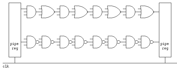
Now, hardware can also be pipelined, for example a parallel multiplier.
Suppose we need to have at most 8 gate delays between pipeline
registers.
Follow an instruction through the piplined architecture.
a few opcodes
The branch slot, programming to avoid delays (filling in nop's):
Note: beq and jump always execute the next physical instruction.
This is called the "delayed branch slot".
if(a==b) x=3; /* simple C code */
else x=4;
y=5;
lw $1,a # possible unoptimized assembly language
lw $2,b # no ($0) shown on memory access
nop # wait for b to get into register 2
nop # wait for b to get into register 2
beq $1,$2,lab1
nop # branch slot, always executed *********
lwim $1,4 # else part
nop # wait for 4 to get into register 1
nop # wait for 4 to get into register 1
sw $1,x # x=4;
j lab2
nop # branch slot, always executed *********
lab1: lwim $1,3 # true part
nop # wait for 3 to get into register 1
nop # wait for 3 to get into register 1
sw $1,x # x=3;
lab2: lwim $1,5 # after if-else, always execute
nop # wait for 5 to get into register 1
nop # wait for 5 to get into register 1
sw $1,y # y=5;
Unoptimized, 20 instructions.
Now, a smart compiler would produce the optimized code:
lw $1,a # possible unoptimized assembly language
lw $2,b # no ($0) shown on memory access
lwim $4,4 # for else part later
lwim $3,3 # for true part later
beq $1,$2,lab1
lwim $5,5 # branch slot, always executed, for after if-else
j lab2
sw $4,x # x=4; in branch slot, always executed !! after jump
lab1: sw $3,x # x=3;
lab2: sw $5,y # y=5;
Optimized, 10 instructions.
The pipeline stage diagram for a==b true is:
1 2 3 4 5 6 7 8 9 10 11 12 clock
lw $1,a IF ID EX MM WB
lw $2,b IF ID EX MM WB
lwim $4,4 IF ID EX MM WB
lwim $3,3 IF ID EX MM WB
beq $1,$2,L1 IF ID EX MM WB assume equal, branch to L1
lwim $5,5 IF ID EX MM WB delayed branch slot
j L2
sw $4,x
L1:sw $3,x IF ID EX MM WB
L2:sw $5,y IF ID EX MM WB
1 2 3 4 5 6 7 8 9 10 11 12
The pipeline stage diagram for a==b false is:
1 2 3 4 5 6 7 8 9 10 11 12 13 clock
lw $1,a IF ID EX MM WB
lw $2,b IF ID EX MM WB
lwim $4,4 IF ID EX MM WB
lwim $3,3 IF ID EX MM WB
beq $1,$2,L1 IF ID EX MM WB assume not equal
lwim $5,5 IF ID EX MM WB
j L2 IF ID EX MM WB jumps to L2
sw $4,x IF ID EX MM WB
L1:sw $3,x
L2:sw $5,y IF ID EX MM WB
1 2 3 4 5 6 7 8 9 10 11 12 13
if(a==b) x=3; /* simple C code */
else x=4;
y=5;
Renaming when there are extra registers that the programmer can
not access (diagram in Alpha below) with multiple units there can be
multiple issue (parallel execution of instructions)
Out of order execution to avoid delays. As seen in the first example,
changing the order of execution without changing the semantics of the
program can achieve faster execution.
There can be multiple issue when there are multiple arithmetic and
other units. This will require significant hardware to detect the
amount of out of order instructions that can be issued each clock.
Now, hardware can also be pipelined, for example a parallel multiplier.
Suppose we need to have at most 8 gate delays between pipeline
registers.
 Note that any and-or-not logic can be converted to use only nand gates
or only nor gates. Thus, two level logic can have two gate delays.
We can build each multiplier stage with two gate delays. Thus we can
have only four multiplier stages then a pipeline register. Using a
carry save parallel 32-bit by 32-bit multiplier we need 32 stages, and
thus eight pipeline stages plus one extra stage for the final adder.
Note that any and-or-not logic can be converted to use only nand gates
or only nor gates. Thus, two level logic can have two gate delays.
We can build each multiplier stage with two gate delays. Thus we can
have only four multiplier stages then a pipeline register. Using a
carry save parallel 32-bit by 32-bit multiplier we need 32 stages, and
thus eight pipeline stages plus one extra stage for the final adder.
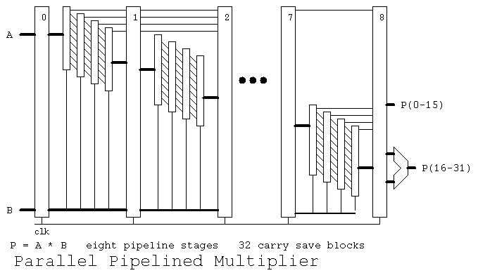 Note that a multiply can be started every clock. Thus a multiply
can be finished every clock. The speedup including the last adder
stage is 9 as shown in:
pipemul_test.vhdl
pipemul_test.out
pipemul.vhdl
A 64-bit PG adder may be built with eight or less gate delays.
The signals a, b and sum are 64 bits. See add64.vhdl for details.
Note that a multiply can be started every clock. Thus a multiply
can be finished every clock. The speedup including the last adder
stage is 9 as shown in:
pipemul_test.vhdl
pipemul_test.out
pipemul.vhdl
A 64-bit PG adder may be built with eight or less gate delays.
The signals a, b and sum are 64 bits. See add64.vhdl for details.
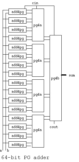 add64.vhdl
Any combinational logic can be performed in two levels with "and" gates
feeding "or" gates, assuming complementation time can be ignored.
Some designers may use diagrams but I wrote a Quine McClusky minimization
program that computes the two level and-or-not VHDL statement
for combinational logic.
quine_mcclusky.c logic minimization
eqn4.dat input data
eqn4.out both VHDL and Verilog output
there are 2^2^N possible functions of N bits
Not as practical, I wrote a Myhill minimization of a finite state machine,
a Deterministic Finite Automata, that inputs a state transition table
and outputs the minimum state equivalent machine. "Not as practical"
because the design of sequential logic should be understandable. The
minimized machine's function is typically unrecognizable.
myhill.cpp state minimization
initial.dfa input data
myhill.dfa minimized output
A reasonably complete architecture description for the Alpha
showing the pipeline is:
basic Alpha
more complete Alpha
The "Cell" chip has unique architecture:
IBM cell architecure
Cell architecture
Some technical data on Intel Core Duo (With some advertising.)
Core Duo all on WEB
From Intel, with lots of advertising:
power is proportional to capacitance * voltage^2 * frequency, page 7.
tech overview
whitepaper
Intel quad core demonstrated
AMD quad core
By 2010 AMD had a 12-core available and Intel had a 8-core available.
and 24 core and 48 core AMD
IBM Power6 at 4.7GHz clock speed
Intel I7 920 Nehalem 2.66GHz not quad $279.99
Intel I7 940 Nehalem 2.93GHz quad core $569.99
Intel I7 965 Nehalem 3.20GHz quad core $999.99
Prices vary with time, NewEgg.com search Intel I7
add64.vhdl
Any combinational logic can be performed in two levels with "and" gates
feeding "or" gates, assuming complementation time can be ignored.
Some designers may use diagrams but I wrote a Quine McClusky minimization
program that computes the two level and-or-not VHDL statement
for combinational logic.
quine_mcclusky.c logic minimization
eqn4.dat input data
eqn4.out both VHDL and Verilog output
there are 2^2^N possible functions of N bits
Not as practical, I wrote a Myhill minimization of a finite state machine,
a Deterministic Finite Automata, that inputs a state transition table
and outputs the minimum state equivalent machine. "Not as practical"
because the design of sequential logic should be understandable. The
minimized machine's function is typically unrecognizable.
myhill.cpp state minimization
initial.dfa input data
myhill.dfa minimized output
A reasonably complete architecture description for the Alpha
showing the pipeline is:
basic Alpha
more complete Alpha
The "Cell" chip has unique architecture:
IBM cell architecure
Cell architecture
Some technical data on Intel Core Duo (With some advertising.)
Core Duo all on WEB
From Intel, with lots of advertising:
power is proportional to capacitance * voltage^2 * frequency, page 7.
tech overview
whitepaper
Intel quad core demonstrated
AMD quad core
By 2010 AMD had a 12-core available and Intel had a 8-core available.
and 24 core and 48 core AMD
IBM Power6 at 4.7GHz clock speed
Intel I7 920 Nehalem 2.66GHz not quad $279.99
Intel I7 940 Nehalem 2.93GHz quad core $569.99
Intel I7 965 Nehalem 3.20GHz quad core $999.99
Prices vary with time, NewEgg.com search Intel I7
<- previous index next ->