<- previous index next ->
"Combinational logic" means gates connected together without feedback.
There is no storage of information. Inputs are applied and outputs
are produced. By convention, we draw combinational logic from
inputs on the left to outputs on the right. For large schematic
diagrams this convention is often violated.
When no constraints are given, any of the gates previously
defined can be connected to design a circuit that performs
the stated function.
Example: Design a circuit that has:
an input for tail lights both on (break pedal in car)
an input for right turn that lets the signal "osc" control right tail light.
an input for left turn that lets the signal "osc" control left tail light.
("osc" will make the light flash on and off as a turn indicator.)
Constraint: use "and" and "or" gates with inversion bubbles allowed
Solution: There are four inputs "tail" "right" "left" and "osc"
There are two outputs "right_light" and "left_light"
The general strategy in design is to work backward from an output.
Yet, as usual, some work from input toward output is also used.
"right_light" must select between "tail" and "osc". Selection
can typically be implemented by "and" gates feeding an "or" gate
with a control signal into one "and" gate and its complement into
the other "and" gate.
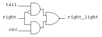 Analyzing this circuit, if "right" is off, "tail" controls
the "right_light". If "right is on, "osc" controls the "right_light".
in VHDL right_light <= (tail and not right) or (right and osc);
tail.vhdl
tail_vhdl.out
in Verilog right_light = (tail & ~right) | (right & osc);
tail.v
tail_v.out
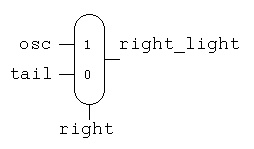
A common symbol for this circuit is a multiplexor, mux for short.
The same circuit as above is usually drawn as the schematic diagram:
Analyzing this circuit, if "right" is off, "tail" controls
the "right_light". If "right is on, "osc" controls the "right_light".
in VHDL right_light <= (tail and not right) or (right and osc);
tail.vhdl
tail_vhdl.out
in Verilog right_light = (tail & ~right) | (right & osc);
tail.v
tail_v.out
A common symbol for this circuit is a multiplexor, mux for short.
The same circuit as above is usually drawn as the schematic diagram:
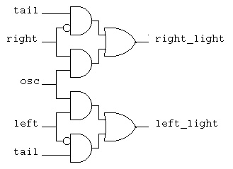
 Now we can use the first schematic with new labeling for
the "left_light", combining the circuits yields:
Now we can use the first schematic with new labeling for
the "left_light", combining the circuits yields:
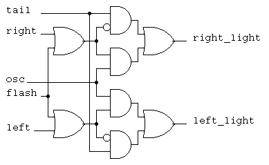
 Now a new requirement is added, the flashers must over ride all
other signals and make "osc" drive both right and left tail lights.
A typical design technique is to build on existing designs,
thus note that "flash" only needs to be able to turn on both
the old "right" and old "left". This is two "or" functions
that are easily added to the previous circuit.
Now a new requirement is added, the flashers must over ride all
other signals and make "osc" drive both right and left tail lights.
A typical design technique is to build on existing designs,
thus note that "flash" only needs to be able to turn on both
the old "right" and old "left". This is two "or" functions
that are easily added to the previous circuit.
 In general a multiplexor can have any number of inputs.
Typically the number of inputs is a power of two and the
control signal, ctl, has the number of bits in the power.
In general a multiplexor can have any number of inputs.
Typically the number of inputs is a power of two and the
control signal, ctl, has the number of bits in the power.
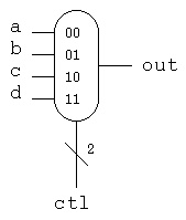 ctl | out Note that "ctl" is a two bit signal, shown by the "2"
----+----
0 0 | a The truth table does not have to expand
0 1 | b a, b, c and d because the mux just passes
1 0 | c the values through to "out" based on the
1 1 | d value of "ctl"
This mux coded in VHDL would be:
entity mux_4 is
port(
a : in std_logic;
b : in std_logic;
c : in std_logic;
d : in std_logic;
ctl : in std_logic vector (1 downto 0));
result : out std_logic;
end entity mux_4;
architecture behavior of mux_4 is
begin -- behavior -- no process needed with concurrent statements
result <= b when ctl='01' else c when ctl='10' else d when ctl='11'
else a after 250 ps;
end architecture behavior; -- of mux_4
This mux coded in verilog would be:
module mux_4to1_assign (
input a,
input b,
input c,
input d,
input ctl,
output out);
assign out = ctl[1] ? (ctl[0] ? d : c) : (ctl[0] ? b : a);
endmodule
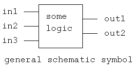
For a general circuit that has some type of description, we use
a rectangle with some notation indicating the function of the
circuit. The inputs and outputs are given signal names.
ctl | out Note that "ctl" is a two bit signal, shown by the "2"
----+----
0 0 | a The truth table does not have to expand
0 1 | b a, b, c and d because the mux just passes
1 0 | c the values through to "out" based on the
1 1 | d value of "ctl"
This mux coded in VHDL would be:
entity mux_4 is
port(
a : in std_logic;
b : in std_logic;
c : in std_logic;
d : in std_logic;
ctl : in std_logic vector (1 downto 0));
result : out std_logic;
end entity mux_4;
architecture behavior of mux_4 is
begin -- behavior -- no process needed with concurrent statements
result <= b when ctl='01' else c when ctl='10' else d when ctl='11'
else a after 250 ps;
end architecture behavior; -- of mux_4
This mux coded in verilog would be:
module mux_4to1_assign (
input a,
input b,
input c,
input d,
input ctl,
output out);
assign out = ctl[1] ? (ctl[0] ? d : c) : (ctl[0] ? b : a);
endmodule
For a general circuit that has some type of description, we use
a rectangle with some notation indicating the function of the
circuit. The inputs and outputs are given signal names.
<- previous index next ->