Different types of buses:
m ISA (Industry Standard Architecture)
m VESA (Video Electronics Standards Association, VL Bus)
m PCI (Peripheral Component Interconnect)
m USB (Universal Serial Bus)
m AGP (Advanced Graphics Port)
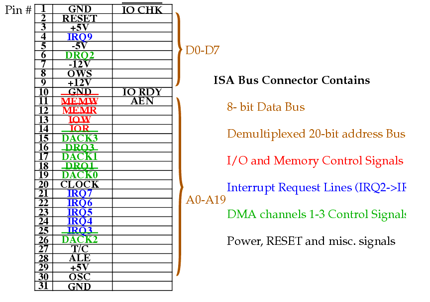
ISA is the oldest of all these and today's computers still have a ISA bus interface in form of an ISA slot (connection) on the main board.
ISA has 8-bit and 16-bit standards along with the 32-bit version (EISA).
All three versions operate at 8MHz.
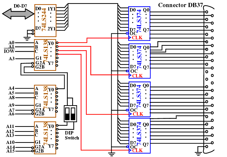
8-Bit ISA Bus Output Interface
8-Bit ISA Bus Output Interface
4, 8-bit latches interfaced using an ISA interface for 32 bit parallel data.
74LS244 buffers used to ensure only
one lower power TTL load on the bus.
Loading is important as many cards can be connected on the bus.
The DIP switch can be used to change the address thus avoiding address conflicts with other cards in the system.
See text for examples of output interface using a PLD and also an ISA bus input interface for A-to-D converters.
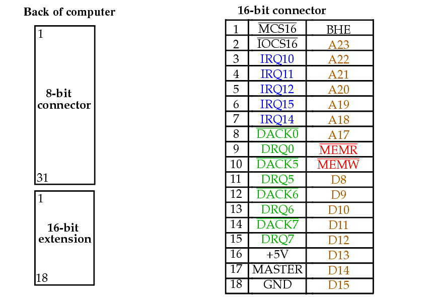
16-bit ISA bus has an additional connector attached behind the 8-bit connector.
Although 8 additional data bits, D
8-D15, are available, the features most often used are the additional interrupt request and DMA request signals.
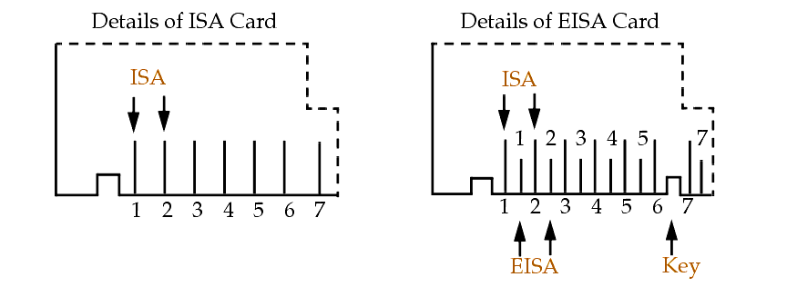
Extended ISA (EISA) has a 32-bit data bus but still operates at 8MHz.
It is rarely used -- mainly as a disk controller or video graphics adapter.
New pins for EISA bus are interspersed with the older pins in the 16-bit ISA connector to preserve compatibility with the old standard.
Most of the new EISA connections are used for the 32-bit data and 32-bit latched address bus.
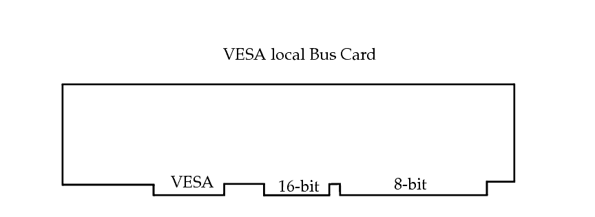
VESA (VL bus) is a 33MHz extension of the ISA bus used of high-speed data transfer applications.
It contains 32-bit address and data bus and is mainly used for video and disk interfaces.
Requires a third connector (VESA connector) to be added behind the standard 16-bit ISA connector.
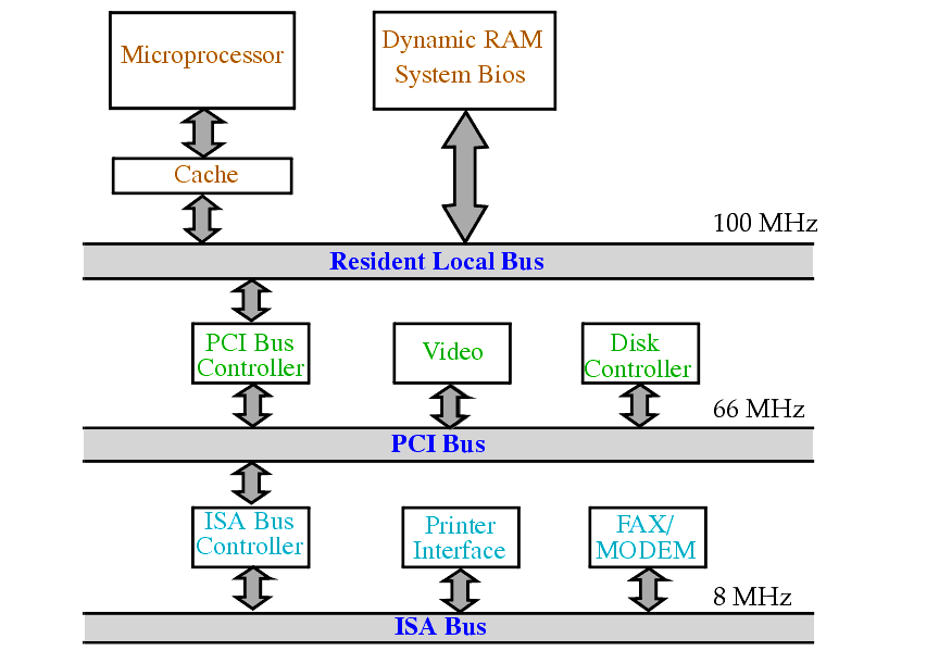
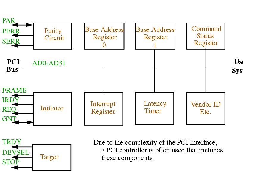
Peripheral Component Interconnect (PCI) Bus
PCI is the most common bus found in computers today due to plug-and-play characteristics and ability to function with 64-bit data bus.
A PCI interface contains a series of registers, located in a small memory device, that contain information about the board.
The information in this registers allow the computer to automatically configure the PCI card (Plug-and-Play
PnP feature).
The microprocessor connects to the PCI bus through an integrated circuit called a
PCI Bridge thus making the PCI bus independent of processor type and architecture.
PCI functions with either a 32-bit or 64-bit address and data bus.
The address and data buses are multiplexed to reduce the size of the edge connector.
Newest versions run at 66 MHz (twice the older 33 MHz version).
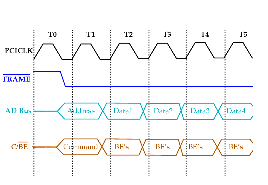
The following commands can appear on the
C/BE pins in cycle T1.
m
I
NTA Sequence: Get the interrupt vector from the interrupt controller. The interrupt vector byte is returned during a read operation.
m
Special Cycle: Used to transfer data to all PCI components, e.g. processor shutdown.
m
I/O Read Cycle: Data are read from an I/O device at address AD0-AD15.
m
I/O Write Cycle: Data are written to an I/O device.
m
Memory Read Cycle: Data are read from memory device.
m
Memory Write Cycle: Data are written to memory device.
m
Configuration Read: Configuration information is read from PCI device
m
Configuration Write: Configuration information is written to PCI device.
m
Memory Multiple Access: Multiple data are read from memory device.
m
Dual Addressing Cycle: Used for transferring data to a 64-bit PCI device which only contains a 32-bit data path.
m
Line Memory Access: Used to read more than two 32-bit numbers.
m
Memory Write with Invalidation: Same as line memory access, but used with write and bypasses write-back function of the cache.
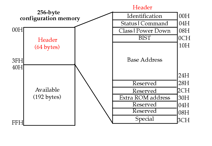
PCI Bus Configuration Space
PCI Bus Configuration Space
The PCI interface contains 256-byte configuration memory that allows plug-and-play feature.
The header holds information about the PCI interface.
The header contains the
unit ID,
vendor ID,
class code and manufacturer defined bits. The vendor ID and class ID are allocated by PCI SIG.
The base address space consists of a base address for the memory, a second for the I/O space and the third for the expansion ROM.
When a PCI bus is present, the system BIOS is extended to support it.
Access to this extended BIOS is through interrupt vector 1AH.
(See text for the currently available functions.)
Once the presence of the BIOS is established, the contents of the configuration memory can be read using other BIOS functions.
PCI Interface Block Diagram
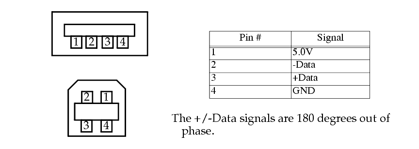
The Universal Serial Bus (USB)
Allows access of up to 127 different connections via a 4 wire serial connection.
This interface is ideal for keyboards, sound cards, modems, etc.
Sound cards can derive their power from an external (no-PC) power supply.
Cable lengths are limited to 5 meters (for the full-speed interface).
Maximum power is given by 100mA x 5V.
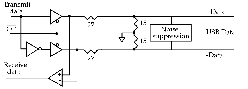
The Universal Serial Bus (USB)
The following circuit can be used to generate the biphase signals.
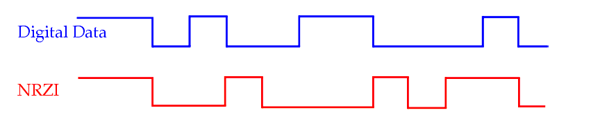
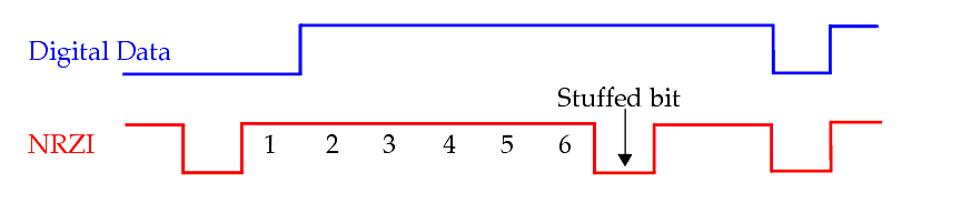
Data packets are sent and received using a NRZI (non-return to zero, inverted) data encoding.
The Universal Serial Bus (USB)
Since the transmitter and receiver must remain synchronized and a large string of 1's do not generate any pulses, a bit may be 'stuffed'.
Here, a bit is added to force a change in the signal line.
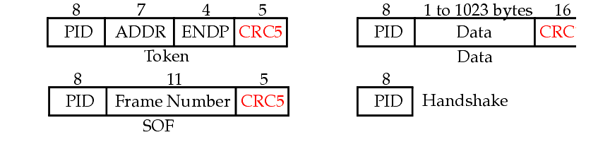
Communication begins with a
sync byte (80H), followed by a packet identification byte (PID).
The PID contains 8 bits -- the rightmost four bits contain the type of packet that follows (if any).
The leftmost 4 bits are the compliment (used for error detection.)
For example, if command is 1000 and 0111 1000 is sent.
The Universal Serial Bus (USB)
PIDs are available for token indicators, data indicators and handshaking:
| PID |
Name |
Type |
Description |
| E1H |
OUT |
Token |
Host->function transaction |
| D2H |
ACK |
Handshake |
Receiver accepts packet |
| C3H |
Data0 |
Data |
Data packet PID even |
| A5H |
SOF |
Token |
Start of Frame |
| 69H |
IN |
Token |
Function -> host transaction |
| 5AH |
NAK |
Handshake |
Receiver does not accept data |
| 4BH |
Data1 |
Data |
Data packet PID odd |
| 3CH |
PRE |
Special |
Host preamble |
| 2DH |
Setup |
Token |
Setup command |
| 1EH |
Stall |
Token |
Stalled |
Formats of the data, token, handshaking and start-of-frame are as follows:
The Universal Serial Bus (USB)
Two types of CRC (cyclic redundancy check):
m 5-bit CRC for tokens, SOF, etc.
Primitive polynomial is X
5 + X
2 + 1
Primitive polynomial is X
16 + X
15 + X
2 + 1
The handshaking PID packets are used to signal errors between the transmitter and receiver.
A NAK causes the transmitter to resend the data.
This is called
stop and wait flow control since the transmitter must wait for an ACK before sending any additional packets.
Operates at system bus speed, e.g. 528M bytes/sec under the 2X compliant system and over 1 G bytes/sec under a 4X.
PCI maximum is ~100 M bytes/sec.