|
|
| PJRC.COM Offline Archive, February 07, 2004 Visit this page on the live site |
| ||
|
Shopping Cart
|
| Home | MP3 Player | 8051 Tools | All Projects | PJRC Store | Site Map |
|
You are here:
8051 Tools
| Search PJRC |
|
|
|
The reset switch and power connector will need to mount to your board somehow. It is much easier to do this before any sockets are in the board. Touching a pair of hanging wires together to reset your system is a poor idea, and pushbuttons are cheap. If a drill is unavailable, usually an ugly but functional hole can be carved in the perf board using a knife. Like the reset switch, a pair of dangling wires should not be used to connect your board to its power supply. A polarized connector is a good investment, which many hobbiests make after their first experience connecting the wires backwards and ruining some or all of the chips on a board. Be sure the power connector is mounted securely. It is usually difficult to "blow" chips if the power connector is polarized and properly mounted, so some time invested here can save $$$ later on.
Once the layout is decided and the reset switch and power are taken care of, the next (optional) step is to glue the sockets to the board. I use epoxy, but a removable glue is also fine. The idea is to mechanically secure the sockets to the board, so that pulling the chips out, handling the board, etc; does not stress the wire wrap connections. It's also a good idea to place stand-offs on the corners of the board, so that when it's sitting on a table, the pins of the sockets don't touch. If the reset switch is a pushbutton type, a standoff should be placed near it so that pressing the button doesn't bend the board.
The last step before wiring is to label the chips and pins on the underside of the board. Be careful, since the pin arrangement will be reversed from the ordinary diagrams, which are top views. You can buy little ID tags to draw your own on labels or tape. The idea is to get the pins labeled, so you don't make mistakes.
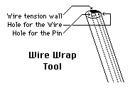 The wire wrap tool has large hole in the center and a small hole on
the side. There is also a wire stripping tool. It is important to
strip off at least one inch (2.5 cm) of the
insulation, perhaps more. Insert the bare wire into the tiny hole
and gently bend the wire where the insulation meets the tool, so
the the wire is roughly at a right angle with the tool. Keeping the
wire in the tool, push the tool onto a pin of a chip and turn, holding
the insulated section of the wire stationary.
Press gently toward the board and continue turning, until all of the stripped wire
is used. This diagram shows basically how it looks:
The wire wrap tool has large hole in the center and a small hole on
the side. There is also a wire stripping tool. It is important to
strip off at least one inch (2.5 cm) of the
insulation, perhaps more. Insert the bare wire into the tiny hole
and gently bend the wire where the insulation meets the tool, so
the the wire is roughly at a right angle with the tool. Keeping the
wire in the tool, push the tool onto a pin of a chip and turn, holding
the insulated section of the wire stationary.
Press gently toward the board and continue turning, until all of the stripped wire
is used. This diagram shows basically how it looks:
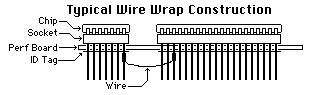
The first things to connect are power, ground, and the decoupling capacitors. It is important to minimize the length of wire between each decoupling capacitor and its nearby chip. If you are good at soldering, it is good to solder each decoupling capacitor under each chip directly to the power pins, but simply using wire wrap is ok as well. You should interconnect your chips' power and ground pins in a grid pattern, not just one long chain. This is usually extra work, but it will reduce noise seen by the chips on the power lines, particularly in the locations farthest from the power connector.
The next thing to connect is the bus lines. It's helpful to use a different color for address and data, but it's even more important to use different color wires for buses and misc signals. Connecting all these wires can take a long time. Boring as it is, be sure to check your work as you go, since starting a group of wires with a mistake can multiply by 8 pretty easily.
After the buses, the other signals are all that's left. These ought to be left until the end, so they will be on top of all the other wires, in the event you want to change them later on.
add photo of some of my wire wrap construction.
![]() Go on to testing and getting it to work.
Go on to testing and getting it to work.