8086/88 Device Specifications
Both are packaged in DIP (Dual In-Line Packages)
m
8086: 16-bit microprocessor with a 16-bit data bus
m
8088: 16-bit microprocessor with an 8-bit data bus
Both are 5V parts (i.e. VDD is 5V)
m
8086: Draws a maximum supply current of 360mA
m
8086: Draws a maximum supply current of 340mA
m
80C86/80C88: CMOS version draws 10mA with temp spec -40 to 225oF
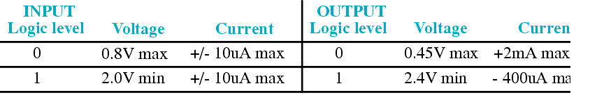
Input/Output current levels:
Yields a 350mV noise immunity for logic 0 (Output max can be as high as 450mV while input max can be no higher than 800mV). This limits the loading on the outputs.
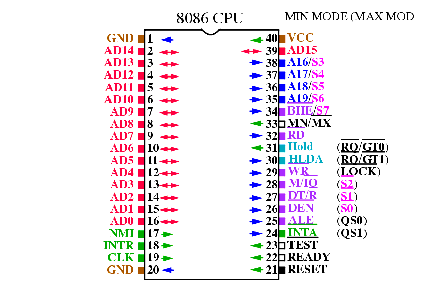
Multiplexed address(ALE=1)/data bus(ALE=0).
m
A19/S6-A16/S3 (multiplexed)
High order 4 bits of the 20-bit address OR status bits S6-S3.
Indicates if address is a Memory or IO address.
When 0, data bus is driven by memory or an I/O device.
Microprocessor is driving data bus to memory or an I/O device. When 0, data bus contains valid data.
m
ALE (Address latch enable)
When 1, address data bus contains a memory or I/O address.
m
DT/R (Data Transmit/Receive)
Data bus is transmitting/receiving data.
Activates external data bus buffers.
m
S7, S6, S5, S4, S3, S2, S1, S0
S7: Logic 1, S6: Logic 0.
S5: Indicates condition of IF flag bits.
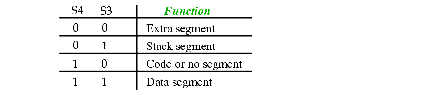
S4-S3: Indicate which segment is accessed during current bus cycle:
S2,
S1,
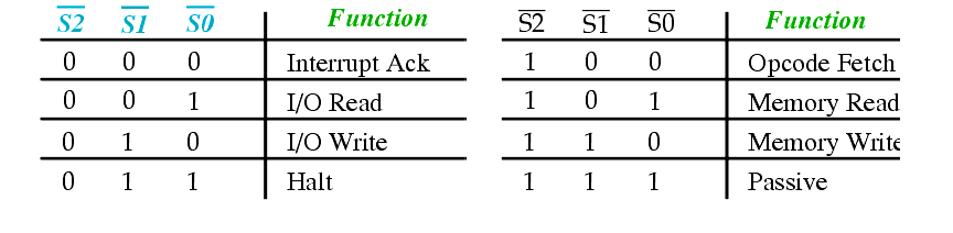
S0: Indicate function of current bus cycle (decoded by 8288).
When 1 and IF=1, microprocessor prepares to service interrupt. INTA
becomes active after current instruction completes.
Interrupt Acknowledge
generated by the microprocessor in response to INTR. Causes the interrupt vector to be put onto the data bus.
Non-maskable interrupt. Similar to INTR except IF flag bit is not consulted and interrupt is vector 2.
Clock input must have a duty cycle of 33% (high for 1/3 and low for 2/3s)
Power supply (5V) and GND (0V)
Select minimum (5V) or maximum mode (0V) of operation.
Bus High Enable. Enables the most significant data bus bits (D15-D8) during a read or write operation.
Used to insert wait states (controlled by memory and IO for reads/writes) into the microprocessor.
Microprocessor resets if this pin is held high for 4 clock periods.
Instruction execution begins at FFFF0H and IF flag is cleared.
An input that is tested by the WAIT instruction.
Commonly connected to the 8087 coprocessor.
Requests a direct memory access (DMA). When 1, microprocessor stops and places address, data and control bus in high-impedance state.
m
HLDA (Hold Acknowledge)
Indicates that the microprocessor has entered the hold state.
Request/grant pins request/grant direct memory accesses (DMA) during maximum mode operation.
Lock output is used to lock peripherals off the system. Activated by using the LOCK: prefix on any instruction.
The queue status bits show status of internal instruction queue. Provided for access by the numeric coprocessor (8087).
m
Peripheral clock signal
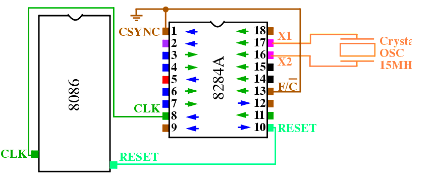
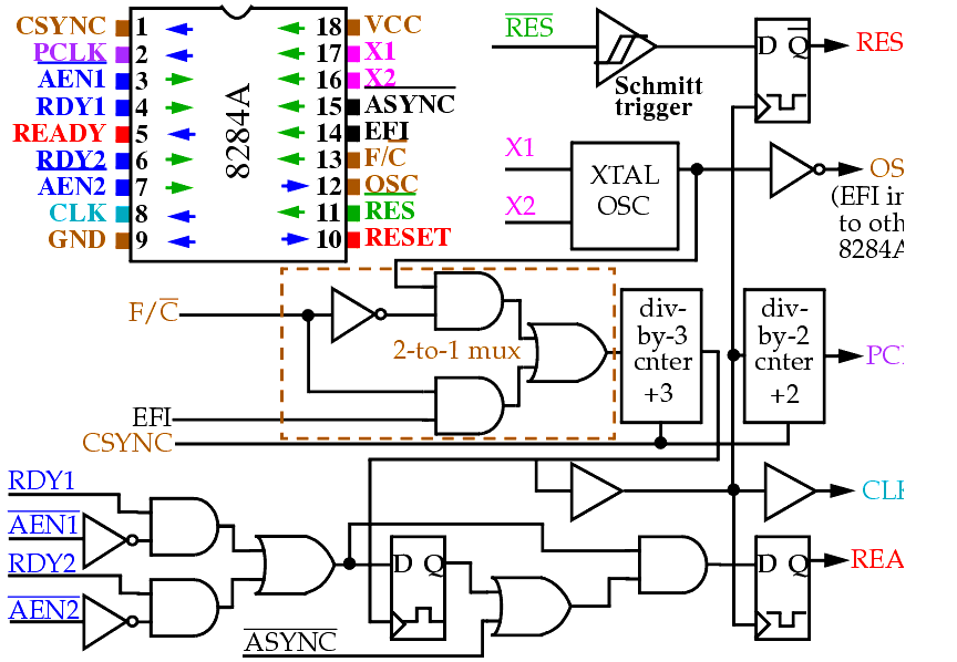
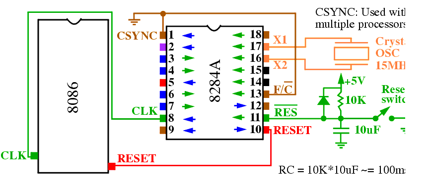
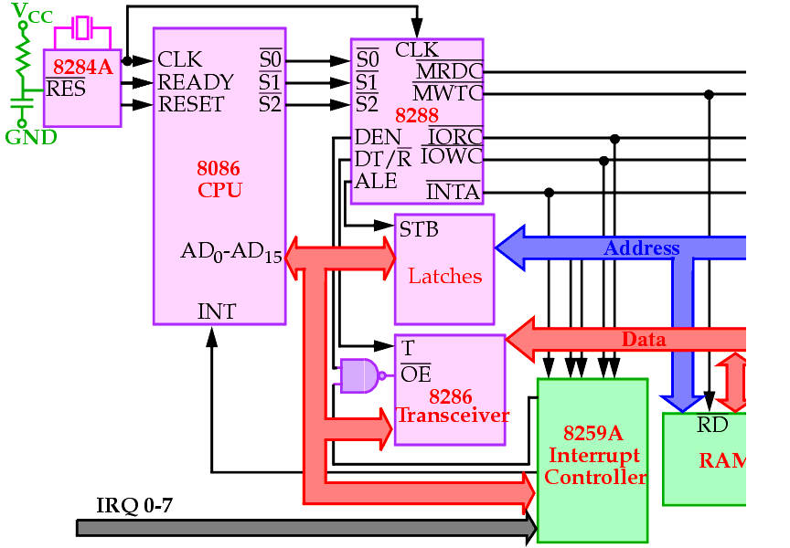
Connection of the 8284 and the 8086.
Crystal is connected to X1 and X2.
XTAL OSC generates square wave signal at crystal's frequency which feeds:
n
An inverting buffer (output OSC) which is used to drive the EFI input of other 8284As.
F/C
selects XTAL or EFI external input.
The MUX drives a divide-by-3 counter (15MHz to 5MHz).
n
The READY flipflop (READY synchronization).
n
A second divide-by-2 counter (2.5MHz clk for peripheral components).
n
CLK which drives the 8086 CLK input.
Negative edge-triggered flipflop applies the RESET signal to the 8086 on the falling edge.
The 8086 samples the RESET pin on the rising edge.
Correct reset timing requires that the RESET input to the microprocessor becomes a logic 1 NO LATER than 4 clocks after power up and stay high for at least 50ms.
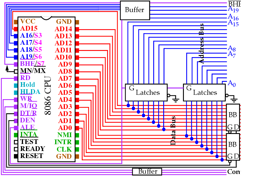
BUS Buffering and Latching
Computer systems have three buses
The Address and Data bus are multiplexed (shared) due to pin limitations on the 8086.
The ALE pin is used to control a set of latches.
All signals MUST be buffered
Buffered Latches for A0-A15.
Control and A16-A19 + BHE are buffered separately.
Data bus buffers must be bi-directional buffers.
In a 8086 system, the memory is designed with two banks
High bank contains the higher order 8-bits and low bank the lower order 8-bits
Data can be transferred as 8 bits from either bank or 16-bits from both
BHE pin selects the high-order memory bank
BUS Buffering and Latching
n
Dump address on address bus.
n
Issue a write (WR
) and set M/IO
to 1.
n
Dump address on address bus.
n
Issue a read (RD
) and set M/IO
to 1.
n
Wait for memory access cycle.
n
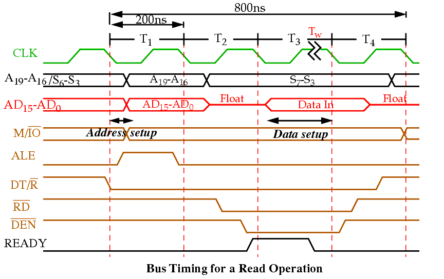
The address is placed on the Address/Data bus.
n
Control signals M/IO
, ALE and DT/R
specify memory or I/O, latch the address onto the address bus and set the direction of data transfer on data bus.
n
8086 issues the RD
or WR
signal, DEN
, and, for a write, the data.
n DEN
enables the memory or I/O device to receive the data for writes and the 8086 to receive the data for reads.
n
This cycle is provided to allow memory to access data.
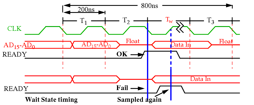
n
READY is sampled at the end of T2.
If low, T3 becomes a wait state.
Otherwise, the data bus is sampled at the end of T3.
n
All bus signals are deactivated, in preparation for next bus cycle.
n
Data is sampled for reads, writes occur for writes.
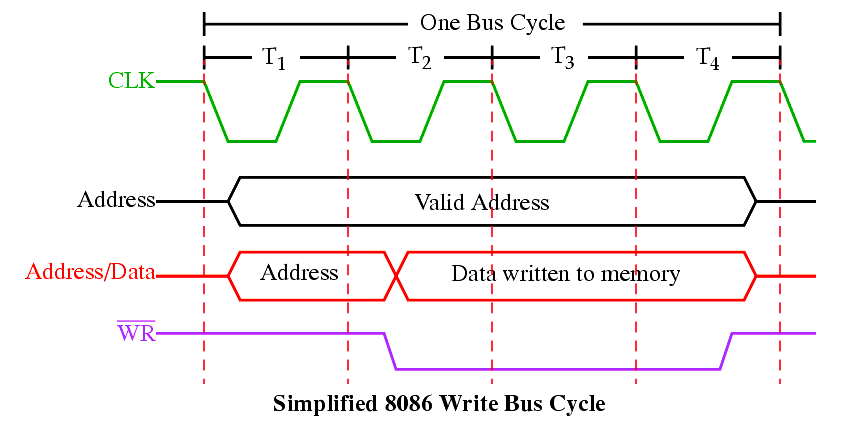
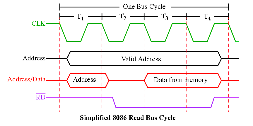
Each BUS CYCLE on the 8086 equals four system clocking periods (T states).
The clock rate is 5MHz,
therefore one Bus Cycle is 800ns.
The transfer rate is 1.25MHz.
Memory specifications (memory access time) must match constraints of system timing.
For example, bus timing for a read operation shows almost 600ns are needed to read data.
However, memory must access faster due to setup times, e.g. Address setup and data setup.
This subtracts off about 150ns.
Therefore, memory must access in at least 450ns minus another 30-40ns guard band for buffers and decoders.
420ns DRAM required for the 8086.
An input to the 8086 that causes wait states for slower memory and I/O components.
A wait state (TW) is an extra clock period inserted between T2 and T3 to lengthen the bus cycle.
For example, this extends a 460ns bus cycle (at 5MHz clock) to 660ns.
Text discusses role of 8284A and timing requirements for the 8086.
Controlled through the MN/MX pin.
n
Minimum mode is cheaper since all control signals for memory and I/O are generated by the microprocessor.
n
Maximum mode is designed to be used when a coprocessor (8087) exists in the system.
Some of the control signals must be generated externally, due to redefinition of certain control pins on the 8086.
The following pins are lost when the 8086 operates in Maximum mode.
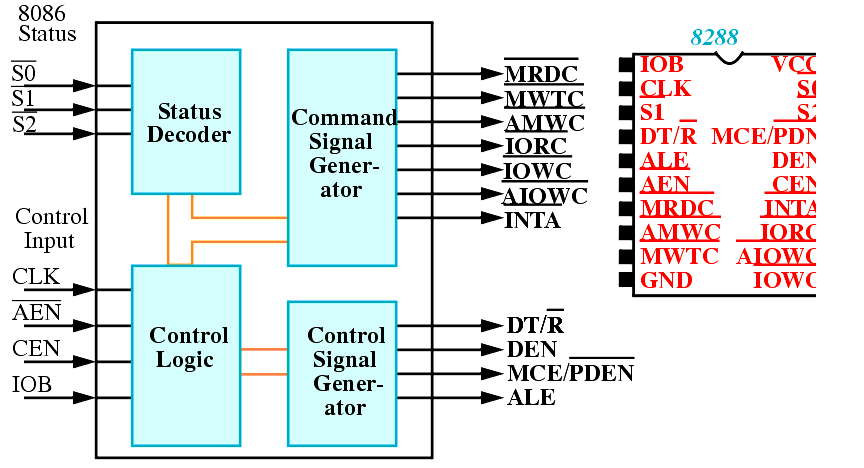
This requires an external bus controller: 8288 Bus Controller.
Separate signals are used for I/O (IORC
and IOWC
) and memory (MRDC
and MWTC
).
Also provided are advanced memory (AIOWC
) and I/O (AIOWC
) write strobes plus INTA
.