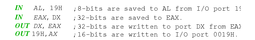
IN and
OUT transfer data between an I/O device and the microprocessor's accumulator (AL, AX or EAX).
The I/O address is stored in:
n Register DX as a 16-bit I/O address (variable addressing).
n The byte, p8, immediately following the opcode (fixed address).
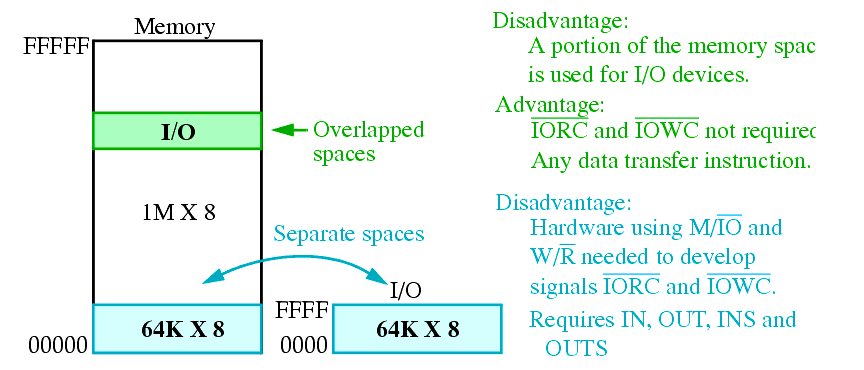
Only 16-bits (A
0 to A
15) are decoded.
Address connections above A
15 are undefined for I/O instructions.
0000H-03XXH are used for the ISA bus.
INS and OUTS transfer to I/O devices using ES:DI and DS:SI, respectively.
Isolated versus Memory-Mapped I/O
Isolated and Memory-Mapped I/O
n In the Isolated scheme, IN, OUT, INS and OUTS are required.
n In the Memory-mapped scheme, any instruction that references memory can be used
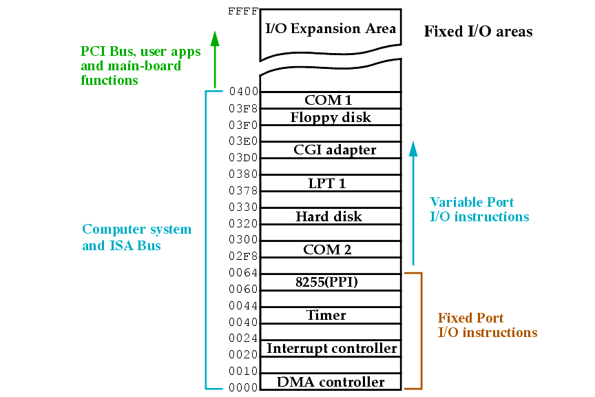
8-bit port addresses used to access system board device, e.g. timer and keyboard.
16-bit port addresses used to access serial and parallel ports, harddrives, etc.
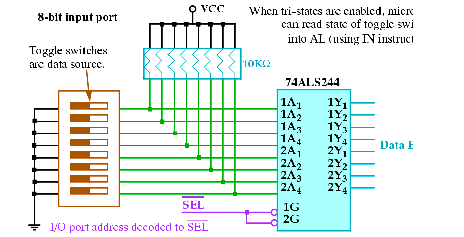
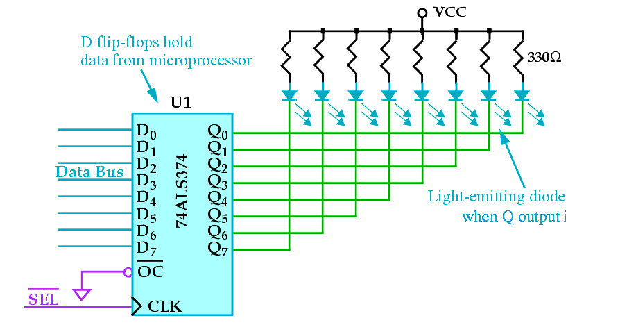
The basic input device (to the microprocessor) is a set of tri-state buffers.
The basic output device (from the microprocessor) is a set of latches.
In this case, the data from the OUT instruction is latched using SEL.
I/O devices are typically slower than the microprocessor.
Handshaking is used to synchronize I/O with the microprocessor.
A device indicates that it is ready for a command or data (through some I/O pin or port).
The processor issues a command to the device, and the device indicates it is busy (not ready).
The I/O device finishes its task and indicates a ready condition, and the cycle continues.
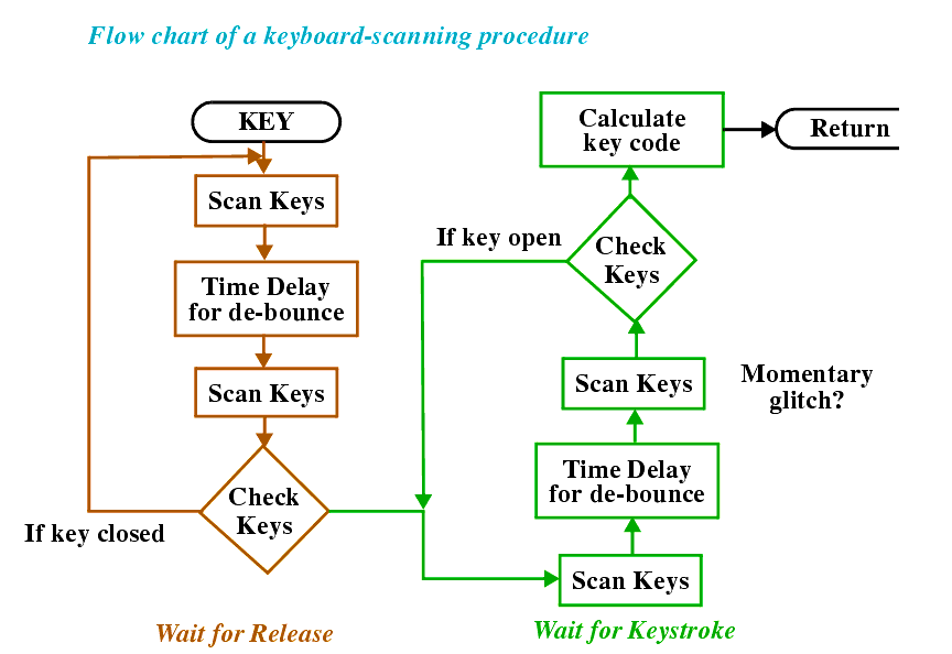
There are two basic mechanisms for the processor to service a device.
n
Polling: Processor initiated. Device indicates it is ready by setting some status bit and the processor periodically checks it.
n
Interrupts: Device initiated. The act of setting a status bit causes an interrupt, and the processor calls an ISR to service the device.
The terminal characteristics of the processor must be matched to those of the I/O devices.
n TTL (0.0V-0.8V low and 2.0-5.0V high) or compatible.
n Switch-based; usually either open or connected.
These must be conditioned before they can be used properly.
For example, to make a simple (single-pole, single-throw) toggle switch TTL compatible:
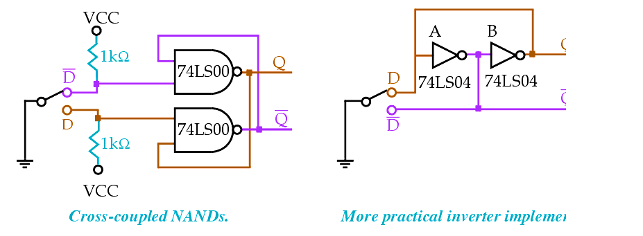
Mechanical switches physically bounce when they are closed (causing them to momentarily open after being closed).
This can cause a problem if they are used as a clocking signal.
Two asynchronous flip-flop solutions are given below:
The basic idea is that these flip-flops store the values even if the D/D nodes both float.
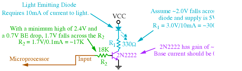
Interfacing an output device requires matching the voltage and current relationships of the devices and processor.
Remember that the standard output levels of TTL compatible devices are 0.0 to 0.4V for logic 0 and 2.4V to 5.0V for logic 1.
The current levels are 0.0 to 2.0mA (logic 0) and 0.0 to -400uA (logic 1).
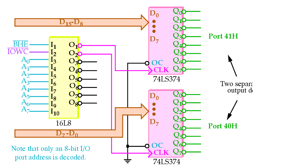
For memory-mapped I/O, decoding is identical to memory decoding.
For isolated I/O, IORC and IOWC are developed using M/IO and W/R pins of the microprocessor.
The text gives examples of 8-bit decoding and 16-bit decoding, which is a straightforward application of devices we've used for memory decoding.
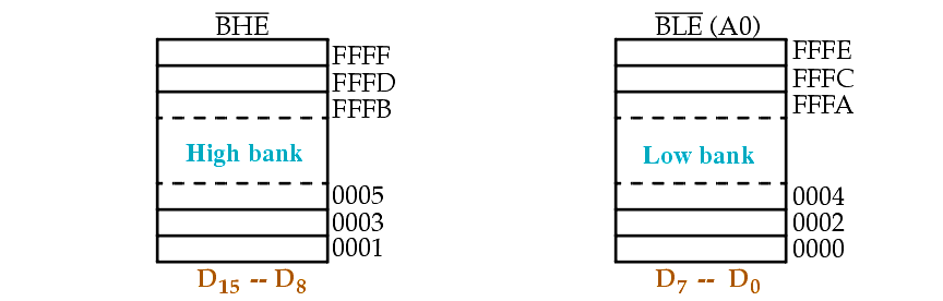
The I/O banks on the 8086 through the 80386SX are also set up like the memory.
Similar to memory writes, any 8-bit I/O write request requires separate write strobes (BHE and BLE) but read requests do not.
Output devices can be 16-bit in which case BHE is not needed.
Input devices can be 8-bit or 16-bit.
Note that instead of latches, high impedance buffers (74ALS244) are used in these cases.
32-bit ports are becoming more popular because of PCI bus primarily.
The EISA and VESA local bus are also 32-bit buses.
For the 64-bit data buses of the Pentium, the I/O ports can appear in any of the 8 banks.
However, only 32-bit transfers are supported, as there are no 64-bit transfer instructions.
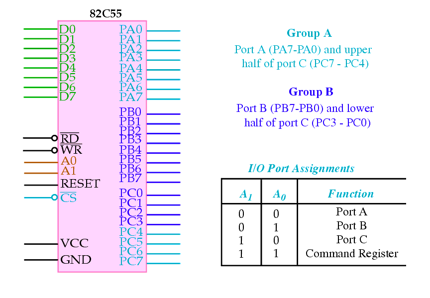
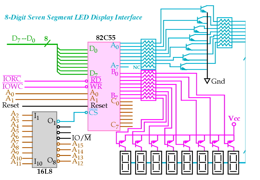
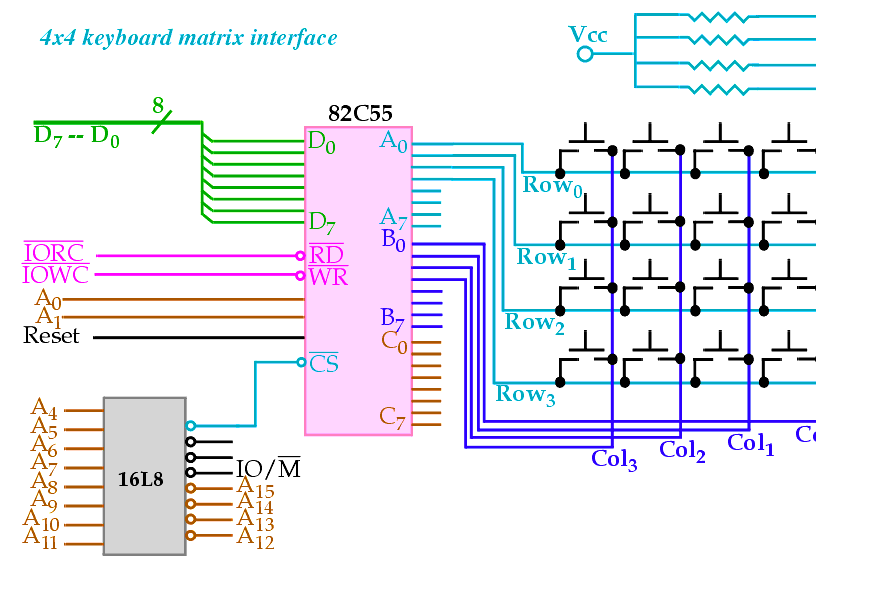
Programmable Peripheral Interface (82C55)
The 82C55 is a popular interfacing component, that can interface any TTL-compatible I/O device to the microprocessor.
It is used to interface to the keyboard and a parallel printer port in PCs (usually as part of an integrated chipset).
Requires insertion of wait states if used with a microprocessor using higher that an 8 MHz clock.
PPI has 24 pins for I/O that are programmable in groups of 12 pins and has three distinct modes of operation.
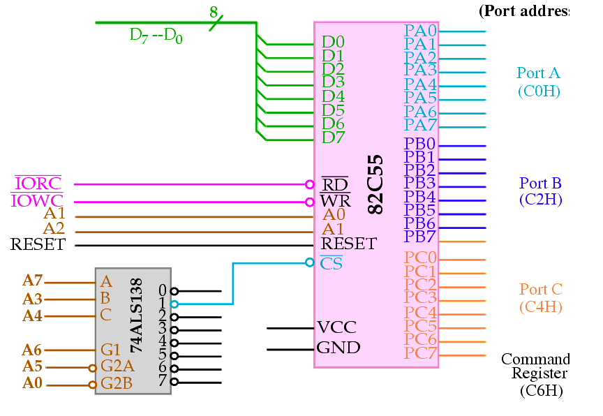
In the PC, an 82C55 or its equivalent is decoded at I/O ports 60H-63H.
Interfacing the 82C55 PPI
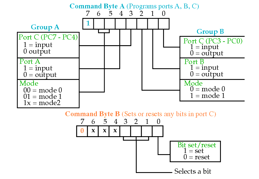
Mode 0 operation causes the 82C55 to function as a buffered input device or as a latched output device.
In previous example, both ports A and B are programmed as (mode 0) simple latched output ports.
Port A provides the segment data inputs to display and port B provides a means of selecting one display position at a time.
Different values are displayed in each digit via fast time multiplexing.
The values for the resistors and the type of transistors used are determined using the current requirements (see text for details).
Textbook has the assembly code fragment demonstrating its use.
Examples of connecting LCD displays and stepper motors are also given.
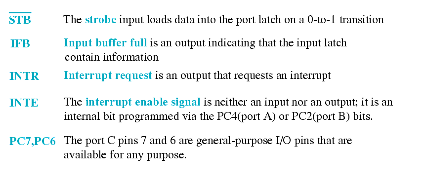
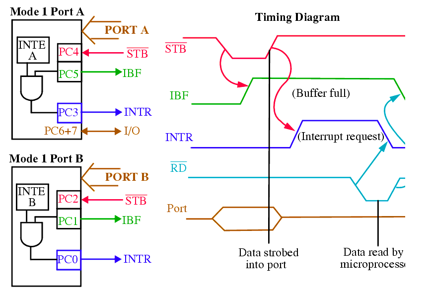
82C55: Mode 1 Strobed Input
Port A and/or port B function as latching input devices. External data is stored in the ports until the microprocessor is ready.
Port C used for control or handshaking signals (cannot be used for data).
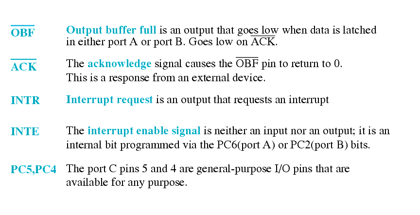
Signal definitions for Mode 1 Strobed Input
82C55: Mode 1 Strobed Input
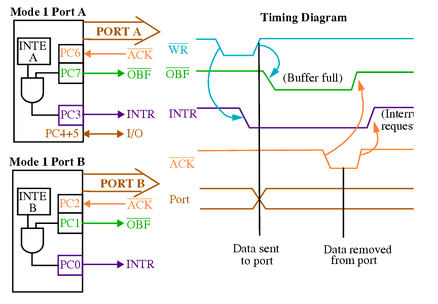
82C55: Mode 1 Strobed Output
Similar to Mode 0 output operation, except that handshaking signals are provided using port C.
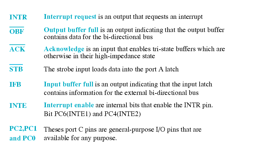
Signal Definitions for Mode 1 Strobed Output
82C55: Mode 1 Strobed Output
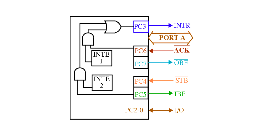
82C55: Mode 2 Bi-directional Operation
Only allowed with port A. Bi-directional bused data used for interfacing
two computers, GPIB interface etc.
82C55: Mode 2 Bi-directional Operation
Timing diagram is a combination of the Mode 1 Strobed Input and Mode 1 Strobed Output Timing diagrams.