DRAM Chip Operating Modes
Memory chips can execute one or more column modes to reduce access time
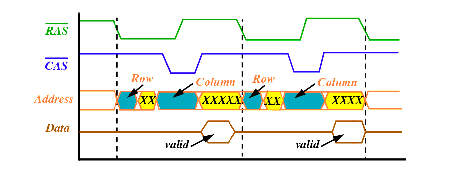
The timing diagram recaps what we have seen before about normal access to the DRAM chips
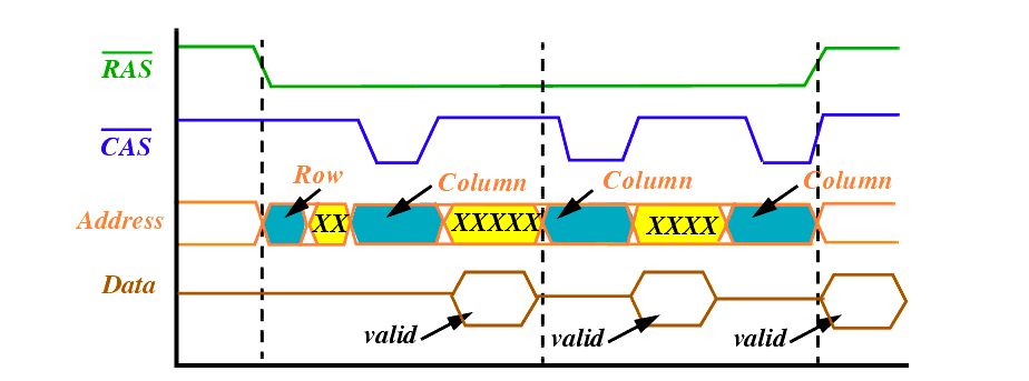
The page mode is a high-speed memory access mode
One the RAS signal is provided to the memory, the whole memory row is read on to the internal data wires
If the next memory access refers to a memory location in the same row but another column, it is not necessary to input and decode the row address again
Thus in page mode, the column address is changed but the row address remains the same
To start read the memory controller activates the RAS signal and transfers the row address
Next the CAS signal is activated and the column address is provided
The RAS signal is not deactivated once the data is read, as in normal mode
Rather the CAS is deactivated for a short time and a new column address is provided and the next CAS strobe
This makes memory accesses faster, the access times is about 50% and the cycle time is about 70% shorter than normal mode
However, this performance increase is only for the second and all subsequent accesses
For stability purpose, the RAS signal cannot remain active for a indefinite period of time
Typically, 200 accesses within the same page can be carried out before the memory controller has to deactivate the RAS signal for one cycle
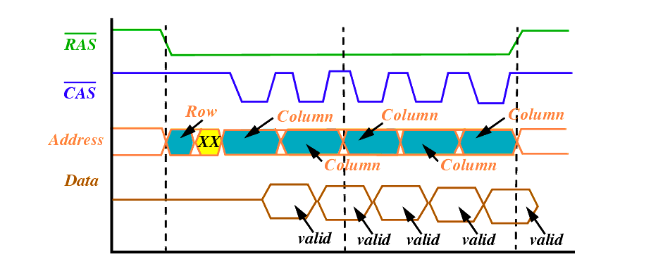
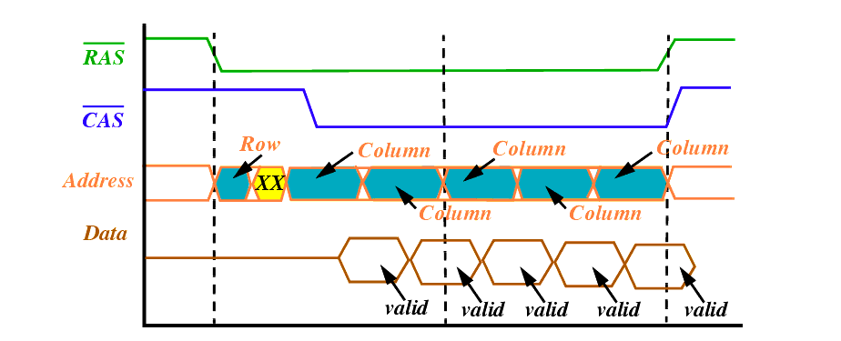
Page mode accesses are not limited to read only as shown on the previous slide
Data may be written in page mode
Read and write operations within the same page can be mixed
Usually RAM is implemented such that a 1MB chip usually has about 1024 locations per page
If memory system is implemented as 32 bits (32 1MB chips) the page is 4Kb
The page size is significant and memory accesses are usually done in blocks close to each other, so page mode is very useful
Hyper Page Mode (EDO Mode)
In hyper page mode, also know as EDO mode, the time between two consecutive CAS activations is shorter than in normal page mode
Column addresses are transferred more quickly, access time is shortened significantly (about 30%) providing higher transfer rates
Very similar to page mode, however CAS is no longer switched.
Only the column address is changed by the DRAM controller and the DRAM logic is intelligent enough to detect the change and provide new data providing more savings
Both CAS and RAS have to be deactivated after a finite period of time
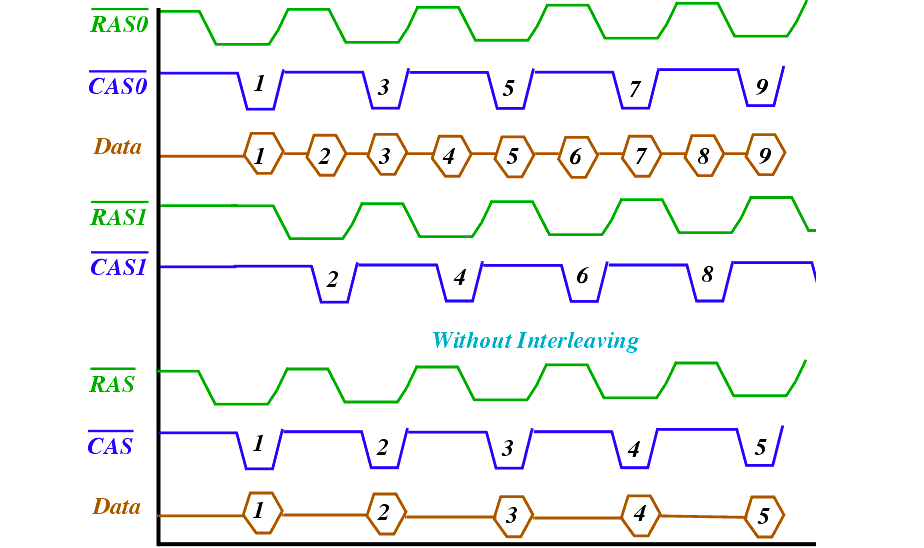
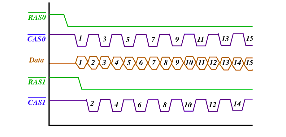
Another way to avoid delays because of the RAS precharge time is memory interleaving
The memory is divided into several banks interleaved at a particular ratio
For e.g., for i386 the memory is 2 way-interleaved
With 2-ways interleaving memory is divided into two banks that are each 32-bit wide (size of the data bus)
All data with even double-word addresses in located in bank 0 and all data with odd double-word addresses in bank 1.
We can still access any byte out of the double-word that we want
However, interleaving is less effective if the program works with byte-sized data
With interleaving, the i386 prefetcher, accesses the two banks alternately
RAS precharge time of one bank overlaps with the access time of the other bank
Interleaving and Page Mode
Page mode can be used in conjunction to interleaving, thus providing even better performance than either stand-alone
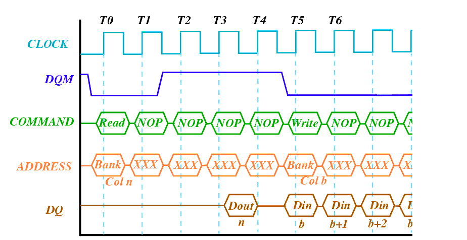
SDRAM: Synchronous DRAM, DDR SDRAM: Double Data Rate SDRAM
(Don't confuse this with SRAM. This is still a dynamic RAM)
SDRAM have typical access time of 8 to 15 ns (even lower now) as compared to the previously discussed EDO RAM which has access time of 50 to 60ns
The difference is noticeable with higher front side bus speeds found in today's boards
For SDRAMs, 168-pin DIMM sockets are used as memory modules with 64 bit data
SDRAMs work in burst mode and with a synchronous clock rate
They do not use the corresponding RAS, CAS, WE and CE signals
Rather commands such as write, read or burst stop are transferred
Some have a EEPROM, which contain data about the module type, organization of the DRAMs used and timing behavior.
Chipset's system management can read this info and configure the best settings
The data transfer rate can be doubled if data is transferred on both the rising and falling edge of the clock signal
This is the principal used for
DDR SDRAMs.
RAMBus
RAMBus modules are know as RIMMs (rambus inline memory modules)
184 contacts, available capacities 64, 128, 256 MB (even bigger available)
The clock speeds are higher, but they use the same concept as DDR SDRAM, transfer data on both the clock edges
As the name,
Bus implies, the entire memory architecture is a bus system.
Consists of the controller on one side, the memory chips (RDRAM) in the middle and a terminator at the other end
Maximum of 32 RDRAM chips can be present per module
No RIMM socket can be left empty, otherwise the bus would be incomplete and nothing would work
Historically RAMBus has been more expensive than DDR SDRAMs, and is used mainly in high end workstations and servers (running with XEON processors)
FLASH memory is very important for today's computer systems
Used as the boot ROM, firmware storage for cards and also as removable storage
Several types of FLASH memories are available, mainly classified by the erasure and storage procedures
The complete storage array is arranged as a single block
Whenever an erase is performed, the contents of all storage locations is cleared
Most modern computers do not use the bulk erase flash devices
Instead a Boot Block FLASH device is used, that provides capabilities to erase individual blocks of storage locations
However, blocks on a boot device are not similar in size
Boot Block FLASH (contd.)
There is a small block called the
boot block
Used mainly to store the boot code for the system
Following this are two small blocks called
parameter blocks
Intended use is to store system parameters, e.g. system configuration table or lookup table
Finally, there are a number of much larger blocks or memory called
main blocks, where the firmware code is stored
Boot block devices are used for a variety of applications that require smaller memory capacity and benefit from the asymmetrical blocking e.g.
in-system programming
This differ from boot block flash in that the memory array is organized into equal sized blocks, with control to erase each block individually
They are referred to as symmetrically blocked and used in design of high-density devices, for large storage of code or data e.g.
FLASH memory drive