8086 - 80386SX 16-bit Memory Interface
These machines differ from the 8088/80188 in several ways:
m The data bus is 16-bits wide.
m The IO/M pin is replaced with M/IO (8086/80186) and MRDC and MWTC for 80286 and 80386SX.
m BHE, Bus High Enable, control signal is added.
m Address pin A0 (or BLE, Bus Low Enable) is used differently.

The 16-bit data bus presents a new problem:
The microprocessor must be able to read and write data to any 16-bit location in addition to any 8-bit location.
The data bus and memory are divided into banks:


8086 - 80386SX 16-bit Memory Interface

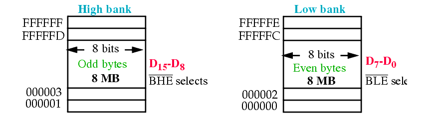
BHE and BLE are used to select one or both:
BHE
BLE
Function
0
0
Both banks enabled for 16-bit transfer
0
1
High bank enabled for an 8-bit transfer
1
0
Low bank enabled for an 8-bit transfer
1
1
No banks selected

Bank selection can be accomplished in two ways:
m Separate write decoders for each bank (which drive CS).
m A separate write signal (strobe) to each bank (which drive WE).
Note that 8-bit read requests in this scheme are handled by the microprocessor (it selects the bits it wants to read from the 16-bits on the bus).

There does not seem to be a big difference between these methods although the book claims that there is.
Note in either method that A0 does not connect to memory and bus wire A1 connects to memory pin A0, A2 to A1, etc.
80386SX 16-bit Memory Interface (Separate Decoders)


Memory Interfaces

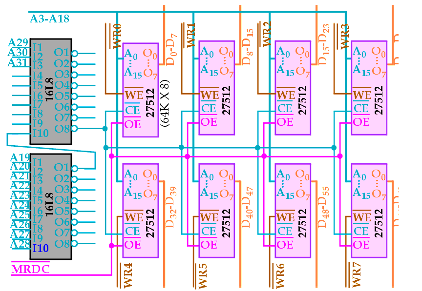
See text for Separate Write Strobe scheme plus some examples of the integration of EPROM and SRAM in a complete system.
It is just an application of what we've been covering.

80386DX and 80486 have 32-bit data buses and therefore 4 banks of memory.
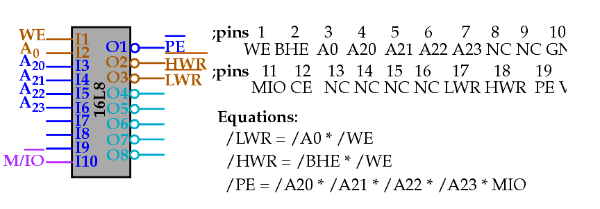
32-bit, 16-bit and 8-bit transfers are accomplished by different combinations of the bank selection signals BE3, BE2, BE1, BE0.

The Address bits A0 and A1 are used within the microprocessor to generate these signals.
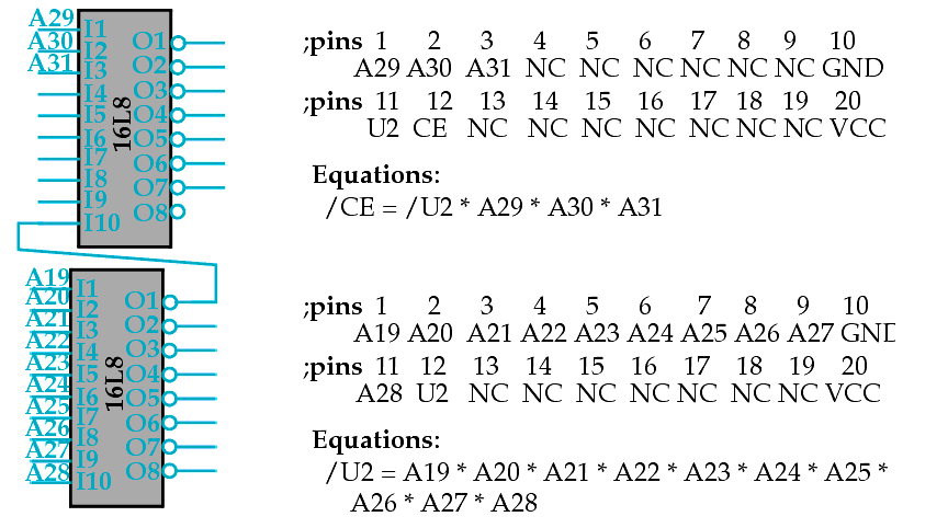
They are don't cares in the decoding of the 32-bit address outside the chip (using a PLD such as the PAL 16L8).

The high clock rates of these processors usually require wait states for memory access.
We will come back to this later.

Pentium Memory Interface

The Pentium, Pentium Pro, Pentium II and III contain a 64-bit data bus.
Therefore, 8 decoders or 8 write strobes are needed as well as 8 memory banks.
The write strobes are obtained by combining the bank enable signals (BEx) with the MWTC signal.
MWTC is generated by combining the M/IO and W/R signals.


Pentium Memory Interface


Pentium Memory Interface

In order to map previous memory into addr. space FFF80000H-FFFFFFFFH


Use a 16L8 to do the WR0 - WR7 decoding using MWTC and BE0 - BE7.
See the text -- Figure 10-35.
Memory Architecture

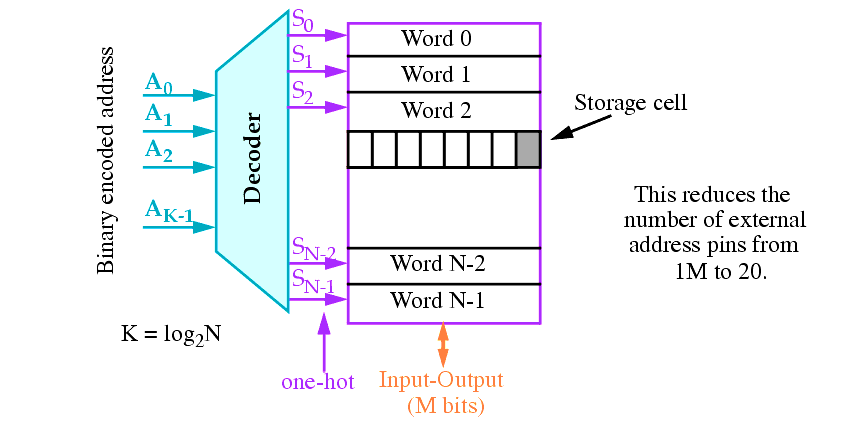
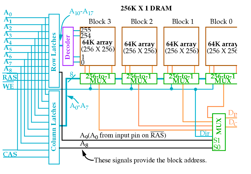
In order to build an N-word memory where each word is M bits wide (typically 1, 4 or 8 bits), a straightforward approach is to stack memory:


This approach is not practical. What can we do?
Memory Architecture
Add a decoder to solve the package problem:


This does not address the memory aspect ratio problem:
The memory is 128,000 time higher than wide (220/23)!
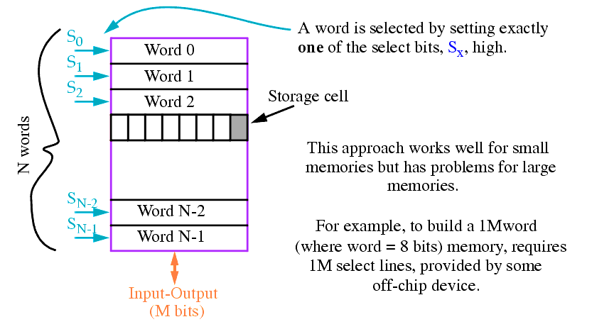
Besides the bizarre shape factor, the design is extremely slow since the vertical wires are VERY long (delay is at least linear to length).
Memory Architecture

The vertical and horizontal dimensions are usually very similar, for an aspect ratio of unity.
Multiple words are stored in each row and selected simultaneously:


Memory Architecture
This strategy works well for memories up to 64 Kbits to 256 Kbits.
Larger memories start to suffer excess delay along bit and word lines.
A third dimension is added to the address space to solve this problem:


Dynamic RAM

DRAM requires refreshing every 2 to 4 ms. (some even at 16ms)
This is due to the storage mechanism. Data is stored as charge on a capacitor
This capacitor is not perfect, i.e., it discharges over the course of time via the access transistor.
Refreshing occurs automatically during a read or write.
Internal circuitry takes care of refreshing cells that are not accessed over this interval.

Three different refresh methods are used:
n RAS-only refresh
n CAS before RAS refresh
n Hidden refresh

Refresh time example:
For a 256K X 1 DRAM with 256 rows, a refresh must occur every 15.6us (4ms/256).
For the 8086, a read or write occurs every 800ns.
This allows 19 memory reads/writes per refresh or 5% of the time.

DRAM Refreshing

RAS-only refresh


Simplest and most widely used method for refreshing, carry out a dummy read cycle

RAS is activated and a row address (refresh address) is applied to the DRAM, CAS inactive

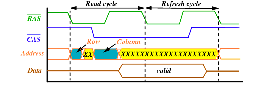
DRAM internally reads one row and amplifies the read data. Not transferred to the output pins as CAS is disabled.

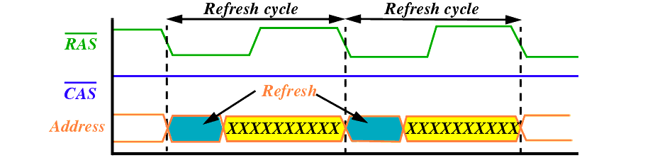
The main disadvantage of this refresh method is that an external logic device, or some program, is required to generate the DRAM row addresses in succession.
DMA chip 8237 (will be discussed later) can be used to generate these addresses
DRAM Refreshing

CAS-before-RAS refresh


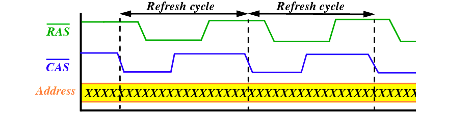
Most modern DRAM chips have one or more internal refresh mode, the most important is the CAS-before-RAS refresh

DRAM chip has its own refresh logic with an address counter
When the above sequence is applied on CAS and RAS the internal refresh logic generates an address and refreshes the associated cells
After every cycle, the internal address counter is incremented

The memory controller just needs to issue the above signals from time-to-time
DRAM Refreshing

Hidden refresh


The more elegant option is the hidden refresh

The actual refresh cycle is hidden behind a normal read access.

During a hidden refresh the CAS signal is further held on a low level, and only the RAS signal is switched

DRAM Refreshing

Hidden refresh

The data read during the read cycle remains valid even while the refresh cycle is in progress

As the time required for a refresh cycle is less than that of a read cycle this saves time

The address counter for refresh cycle is in the DRAM, the row and column addresses shown in the timing diagram are only for the read cycle

If the CAS signal stays low for a sufficiently long time, several refresh cycles can be carried out in succession by switching the RAS signal frequently between 0 and 1

Most new motherboards implement the option of refreshing the DRAM memory with the CAS-before-RAS or hidden refresh instead of using the DMA chip and the timer chip (as done for older 8086 systems)
Dynamic RAM


DRAM Controllers

A DRAM controller is usually responsible for address multiplexing and generation of the DRAM control signals.

These devices tend to get very complex. We will focus on a simpler device, the Intel 82C08, which can control two banks of 256K X 16 DRAM memories for a total of 1 MB.

Microprocessor bits A1 through A18 (18 bits) drive the 9 Address Low (AL) and 9 Address High (AH) bits of the 82C08. 9 of each of these are strobed onto the address wires A0 through A8 to the memories.

Either RAS0/CAS0 or RAS1/CAS1 are strobed depending on the address.
This drives a 16-bit word onto the High and Low data buses (if WE is low) or writes an 8 or 16 bit word into the memory otherwise.
DRAM Controllers


DRAM Controllers

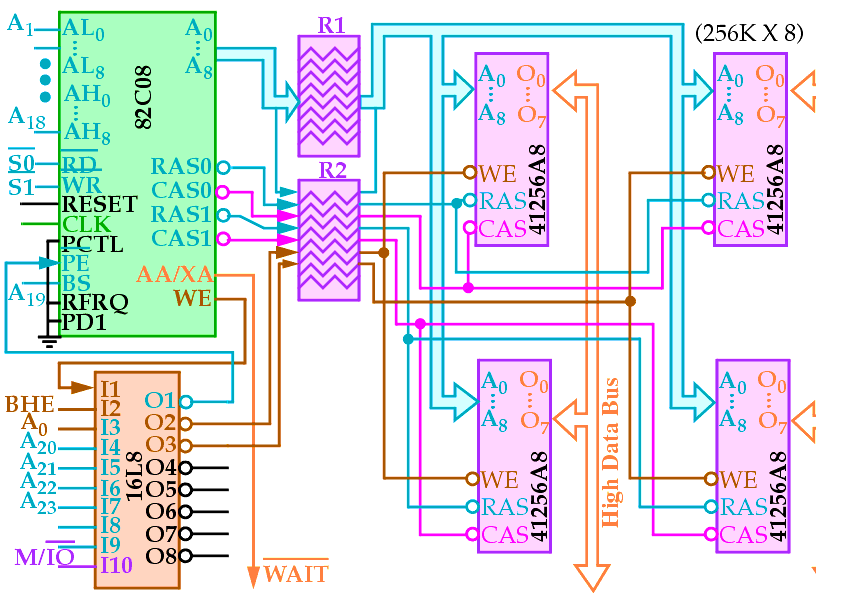
WE (from the 82C08), BHE and A0 are used to determine if a write is to be performed and which byte(s) (low or high or both) is to be written.

Address bit A20 through A23 along with M/IO enable these memories to map onto 1 MByte range (000000H-0FFFFFH).

16L8 Programming: