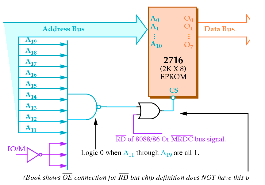
The processor can usually address a memory space that is much larger than the memory space covered by an individual memory chip.
In order to splice a memory device into the address space of the processor, decoding is necessary.
For example, the 8088 issues 20-bit addresses for a total of 1MB of memory address space.
However, the BIOS on a 2716 EPROM has only 2KB of memory and 11 address pins.
A decoder can be used to decode the additional 9 address pins and allow the EPROM to be placed in any 2KB section of the 1MB address space.
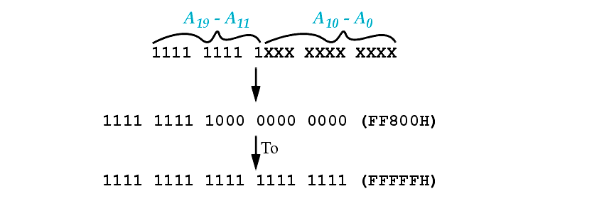
To determine the address range that a device is mapped into:
This 2KB memory segment maps into the reset location of the 8086/8088 (FFFF0H).
NAND gate decoders are not often used
Large fan-in NAND gates are not efficient
Multiple NAND gate IC's might be required to perform such decoding
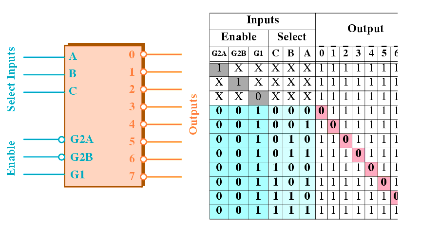
Rather the 3-to-8 Line Decoder (74LS138) is more common.
The 3-to-8 Line Decoder (74LS138)
Note that all three Enables (G2A, G2B, and G1) must be active, e.g. low, low and high, respectively.
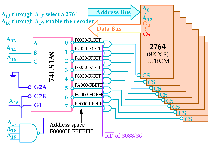
Each output of the decoder can be attached to an 2764 EPROM (8K X 8).
The EPROMs cover a 64KB section of memory.
Yet a third possibility is a PLD (Programmable Logic Device).
PLDs come in three varieties:
n
PLA (Programmable Logic Array)
n
PAL (Programmable Array Logic)
n
GAL (Gated Array Logic)
PLDs have been around since the mid-1970s but have only recently appeared in memory systems (PALs have replaced PROM address decoders).
PALs and PLAs are fuse-programmed (like the PROM).
Some are erasable (like the EPROM).
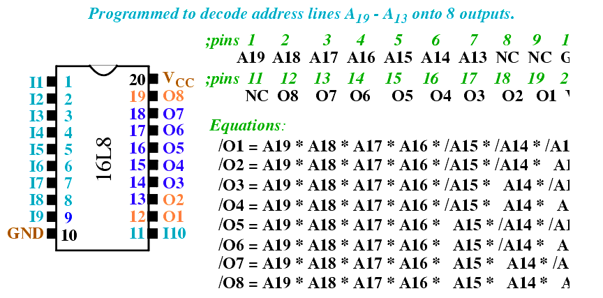
A PAL example (16L8) is shown in the text and is commonly used to decode the memory address, particularly for 32-bit addresses generated by the 80386DX and above.
It has 10 fixed inputs (Pins 1-9, 11), two fixed outputs (Pins 12 and 19) and 6 pins that can be either (Pins 13-18).
AND/NOR device with logic expressions (outputs) with up to 16 ANDed inputs and 7 ORed product terms.
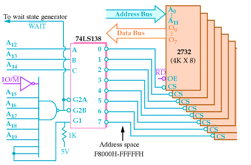
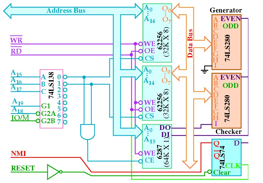
8088 and 80188 (8-bit) Memory Interface
The memory systems sees the 8088 as a device with:
n
20 address connections (A19 to A0).
n
8 data bus connections (AD7 to AD0).
n
3 control signals, IO/M, RD, and WR.
We'll look at interfacing the 8088 with:
n
32K of EPROM (at addresses F8000H through FFFFFH).
n
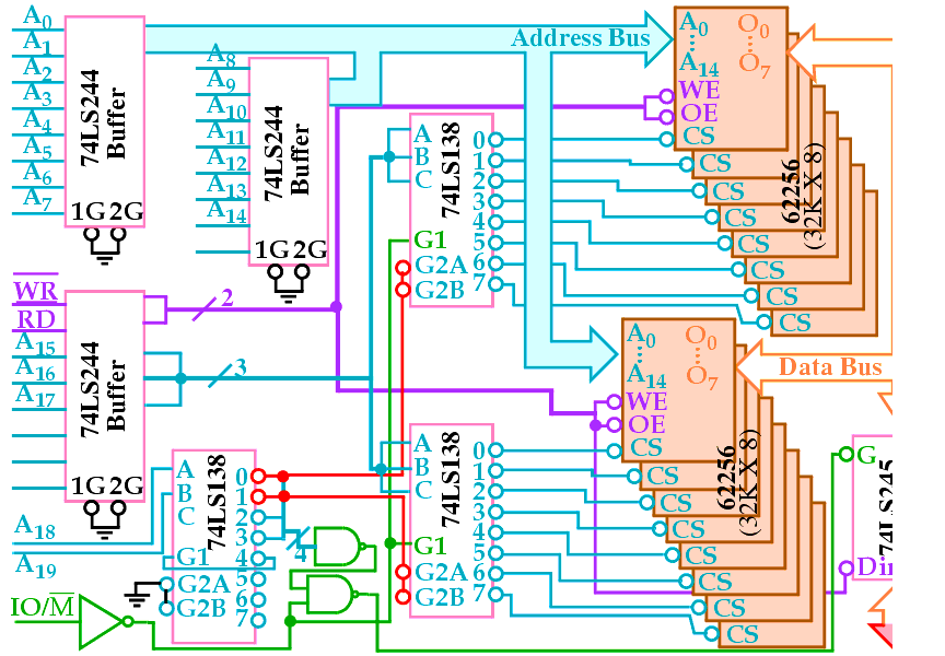
512K of SRAM (at addresses 00000H through 7FFFFH).
The EPROM interface uses a 74LS138 (3-to-8 line decoder) plus 8 2732 (4K X 8) EPROMs.
The EPROM will also require the generation of a wait state.
The EPROM has an access time of 450ns.
The 74LS138 requires 12ns to decode.
The 8088 runs at 5MHz and only allows 460ns for memory to access data.
A wait state adds 200ns of additional time.
8088 and 80188 (8-bit) EPROM Memory Interface
The 8088 cold starts execution at FFFF0H. JMP to F8000H occurs here.
8088 and 80188 (8-bit) RAM Memory Interface
8088 and 80188 (8-bit) RAM Memory Interface
The 16 62256s on the previous slide are actually SRAMs.
Access times are on order of 10ns.
Flash memory can also be interfaced to the 8088 (see text).
However, the write time (400ms!) is too slow to be used as RAM (as shown in the text).
Parity checking is used to detect single bit errors in the memory.
The current trend is away from parity checking.
Parity checking adds 1 bit for every 8 data bits.
n
For EVEN parity, the 9th bit is set to yield an even number of 1's in all 9 bits.
n
For ODD parity, the 9th bit is set to make this number odd.
For 72-pin SIMMs, the number of data bits is 32 + 4 = 36 (4 parity bits).
Parity for Memory Error Detection
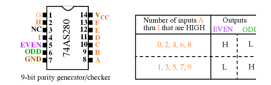
74AS280 Parity Generator/Checker
This circuit generates EVEN or ODD parity for the 9-bit number placed on its inputs.
Typically, for generation, the 9th input bit is set to 0.
This circuit also checks EVEN or ODD parity for the 9-bit number.
In this case, the 9th input bit is connected to the 9th bit of memory.
For example, if the original byte has an even # of 1's (with 9th bit at GND), the parity bit is set to 1 (from the EVEN output).
If the EVEN output goes high during the check, then an error occurred.
Parity for Memory Error Detection
This parity scheme can only detect a single bit error.
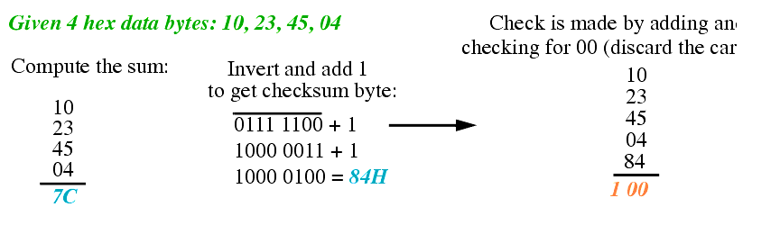
Block-Check Character (BCC) or Checksum.
Can detect multiple bit errors.
This is simply the two's complement sum (the negative of the sum) of the sequence of bytes.
No error occurred if adding the data values and the checksum produces a 0.
If 45 changes to 44 AND 04 changes to 05, the error is missed.
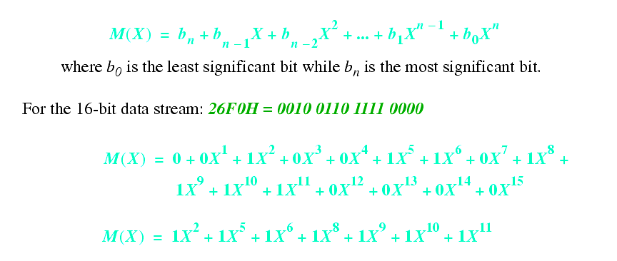
Cyclic Redundancy Check (CRC)
Commonly used to check data transfers in hardware such as harddrives.
Treats data as a stream of serial data n-bits long.
The bits are treated as coefficients of a characteristic polynomial, M(X) of the form:
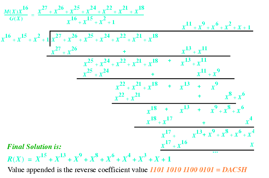
Cyclic Redundancy Check (CRC) (cont.)
The CRC is found by applying the following equation.
G(X) is the called the generator polynomial and has special properties.
A commonly used polynomial is:
The remainder R(X) is appended to the data block.
When the CRC and R(X) is computed by the receiver, R(X) should be zero.
Since G(X) is of power 16, the remainder, R(X), cannot be of order higher than 15.
Therefore, no more than 2 bytes are needed independent of the data block size.
Cyclic Redundancy Check (CRC) (cont.)
Parity, BCC and CRC are only mechanisms for error detection.
The system is halted if an error is found in memory.
Error correction is starting to show up in new systems.
SDRAM has ECC (Error Correction Code).
Correction will allow the system can continue operating.
If two errors occur, they can be detected but not corrected.
Error correction will of course cost more in terms of extra bits.
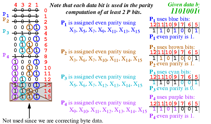
Error correction is based on Hamming Codes.
There is lots of theory here but our focus will be on implementation.
The objective is to correct any single bit errors in an 8-bit data byte.
In other words, we need 4 parity bits to correct single bit errors.
Note that the parity bits are at bit positions that are powers of 2.
P1 is generated by computing the parity of X3, X5, X7, X9, X11, X13, X15.
These numbers have a 1 in bit position 1 of the subscript in binary.
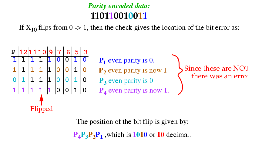
Parity for Memory Error Correction
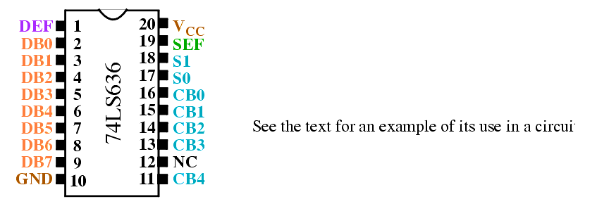
The 74LS636 corrects errors by storing 5 parity bits with each byte of data.