Lab 8: SR-Latch

Table of Contents
Objective and Overview
In this lab, you will be verifying the operation of a simple synchronous SR-latch, starting from modeling an asynchronous S-R latch.
Required Equipment
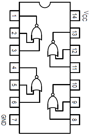
- 7402: Quad 2-input NOR IC
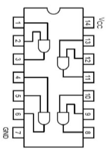
- 7408: Quad 2-input AND IC
- 2 LEDs
- 1 Quad Switch
- 2 Resistors 330Ω
- 4 resistors - 10kΩ
Discussion and Theory
The SR-latch is one of the simplest sequential logic structures. It employs positive feedback (two inversions), and consists of two NOR gates as shown in the following figure. To study it’s behaviour in Verilog we’ll use delay modeling to explore the latch behavior before the lab.
Verilog and Naive Unit Delay
Previously you learned about
- instantiating Verilog primitives (e.g. not, and, or, xor)
- defining Verilog Modules
- creating Verilog Testbenches
- using Icarus Verilog to perform simulations
- inserting a monitor statements to print signal changes and times
- saving a waveform as a value change dump file
A new skill we will learn today is to add delays to allow us to see signal propagation along a combinational path and then use it in a sequential circuit to observe latching behavior.
Delays in physical circuits are dependent on the type of gate, number of inputs (fan-in), and load (which is based on factors such as the number of gates being driven, also called fan-out). We will intially assume all gates have input-to-output propagation delay of 1 time unit.
The delay modeling feature in Verilog is more accurate modeling of real circuits. In real circuits, delay is either an unwanted characteristic or it is fundamentally required for the function of the physical circuit. Here is a simple interactive depiction of an inverter without and with delay.
Next we’ll examine and compare code without and then with delays added to understand how to add delay in your Verilog Code. It will be added to the instantiations.
Example code without delay:
module sop_nodelay(a,b,c,y); // Sum of Products, y=f(a,b,c)
  input logic a,b,c;
  output logic y;
  logic a_n,b_n,c_n;
  not not00(a_n,a);
  not not01(b_n,b);
  not not02(c_n,c);
  and and00(p0, a, b);
  and and01(p1,b, c_n);
  or or00(y,p0,p1);
endmodule
Since Verilog primitives don’t have any default delay, all internal signals and the output will appear to change at the same time in simulation.
How to specify delay?
To add the naive delay of 1 time unit to all gates, include #1 to the primitive instantiations as in the following module.
Also note the code that in on the first line:
`timescale 1ns / 100ps
This specifies that the default time unit and time resolution will be 1 ns, meaning that #1 will correspond to 1 ns. It also specifies the the time resolution is 100ps – so for instance #1.3 could be used to specify 1.3 ns, but #1.31 is also 1.3 ns. We will only use #1 for simplicity and call this a naive unit delay.
`timescale 1ns / 100ps
// Sum of Products, y=f(a,b,c)
module sop_naivedelay(y,a,b,c);
  input a,b,c;
  output logic y;
  logic a_n,b_n,c_n,p0,p1;
  not #1 not00(a_n,a);
  not #1 not01(b_n,b);
  not #1 not02(c_n,c);
  and #1 and00(p0, a, b);
  and #1 and01(p1,b, c_n);
  or #1 or00(y,p0,p1);
endmodule
Here is a Testbench that you can use to perform the simulation and observe the signal propagation along a path:
`timescale 1ns / 100ps
module sop_naivedelay_tb;
    // Variables for Testbench to drive DUT Inputs
    logic a_tb,b_tb,c_tb;
    // Nets from DUT outputs
    logic y_tb;

    // DUT (device under test
    // instantiate the module to test here:
    sop_naivedelay DUT (.y(y_tb),.a(a_tb),.b(b_tb),.c(c_tb));

    initial begin
    $monitor($time,
             " TB: y=%1b,a=%1b,b=%1b,c=%1b DUT:a_n=%1b,b_n=%1b,c_n=%1b,p0=%1b,p1=%1b",
                           y_tb,a_tb,b_tb,c_tb,DUT.a_n,DUT.b_n,DUT.c_n,DUT.p0,DUT.p1);
              //note use of hierarchical signal referencing DUT.01

        $dumpfile("test.vcd");
    $dumpvars(0,sop_naivedelay_tb);  ////

    a_tb =0; b_tb=0; c_tb = 0;
    #10
    a_tb =0; b_tb=0; c_tb = 1;
    #10
    a_tb =0; b_tb=1; c_tb = 0;
    #10
    a_tb =0; b_tb=1; c_tb = 1;
    #10
    a_tb =1; b_tb=0; c_tb = 0;
    #10
    a_tb =1; b_tb=0; c_tb = 1;
    #10
    a_tb =1; b_tb=1; c_tb = 0;
    #10
    a_tb =1; b_tb=1; c_tb = 1;


    #100;
      $finish; // can alternatively use $stop to
              //  interact with the simulation instead of closing it.

    end

endmodule
Here is the expected output. The input are changed at multiples of 10 ns.
Look at the effect of the input change at 20 ns.
The output of the NOT gate changes at 21 ns
The output of AND gate changes at 22 ns.
The output of the OR gate changes 23 ns.
0 TB: y=x,a=0,b=0,c=0 DUT:a_n=z,b_n=z,c_n=z,p0=z,p1=z
1 TB: y=x,a=0,b=0,c=0 DUT:a_n=1,b_n=1,c_n=1,p0=0,p1=0
2 TB: y=0,a=0,b=0,c=0 DUT:a_n=1,b_n=1,c_n=1,p0=0,p1=0
10 TB: y=0,a=0,b=0,c=1 DUT:a_n=1,b_n=1,c_n=1,p0=0,p1=0
11 TB: y=0,a=0,b=0,c=1 DUT:a_n=1,b_n=1,c_n=0,p0=0,p1=0
20 TB: y=0,a=0,b=1,c=0 DUT:a_n=1,b_n=1,c_n=0,p0=0,p1=0
21 TB: y=0,a=0,b=1,c=0 DUT:a_n=1,b_n=0,c_n=1,p0=0,p1=0
22 TB: y=0,a=0,b=1,c=0 DUT:a_n=1,b_n=0,c_n=1,p0=0,p1=1
23 TB: y=1,a=0,b=1,c=0 DUT:a_n=1,b_n=0,c_n=1,p0=0,p1=1
30 TB: y=1,a=0,b=1,c=1 DUT:a_n=1,b_n=0,c_n=1,p0=0,p1=1
31 TB: y=1,a=0,b=1,c=1 DUT:a_n=1,b_n=0,c_n=0,p0=0,p1=1
32 TB: y=1,a=0,b=1,c=1 DUT:a_n=1,b_n=0,c_n=0,p0=0,p1=0
33 TB: y=0,a=0,b=1,c=1 DUT:a_n=1,b_n=0,c_n=0,p0=0,p1=0
40 TB: y=0,a=1,b=0,c=0 DUT:a_n=1,b_n=0,c_n=0,p0=0,p1=0
41 TB: y=0,a=1,b=0,c=0 DUT:a_n=0,b_n=1,c_n=1,p0=0,p1=0
50 TB: y=0,a=1,b=0,c=1 DUT:a_n=0,b_n=1,c_n=1,p0=0,p1=0
51 TB: y=0,a=1,b=0,c=1 DUT:a_n=0,b_n=1,c_n=0,p0=0,p1=0
60 TB: y=0,a=1,b=1,c=0 DUT:a_n=0,b_n=1,c_n=0,p0=0,p1=0
61 TB: y=0,a=1,b=1,c=0 DUT:a_n=0,b_n=0,c_n=1,p0=1,p1=0
62 TB: y=1,a=1,b=1,c=0 DUT:a_n=0,b_n=0,c_n=1,p0=1,p1=1
70 TB: y=1,a=1,b=1,c=1 DUT:a_n=0,b_n=0,c_n=1,p0=1,p1=1
71 TB: y=1,a=1,b=1,c=1 DUT:a_n=0,b_n=0,c_n=0,p0=1,p1=1
72 TB: y=1,a=1,b=1,c=1 DUT:a_n=0,b_n=0,c_n=0,p0=1,p1=0
Done
These delays can also be explored visually in by generating a .vcd file and using a waveform viewer.
You should use GTKwave to observe the output.
SR-latch: asynchronous and synchronous
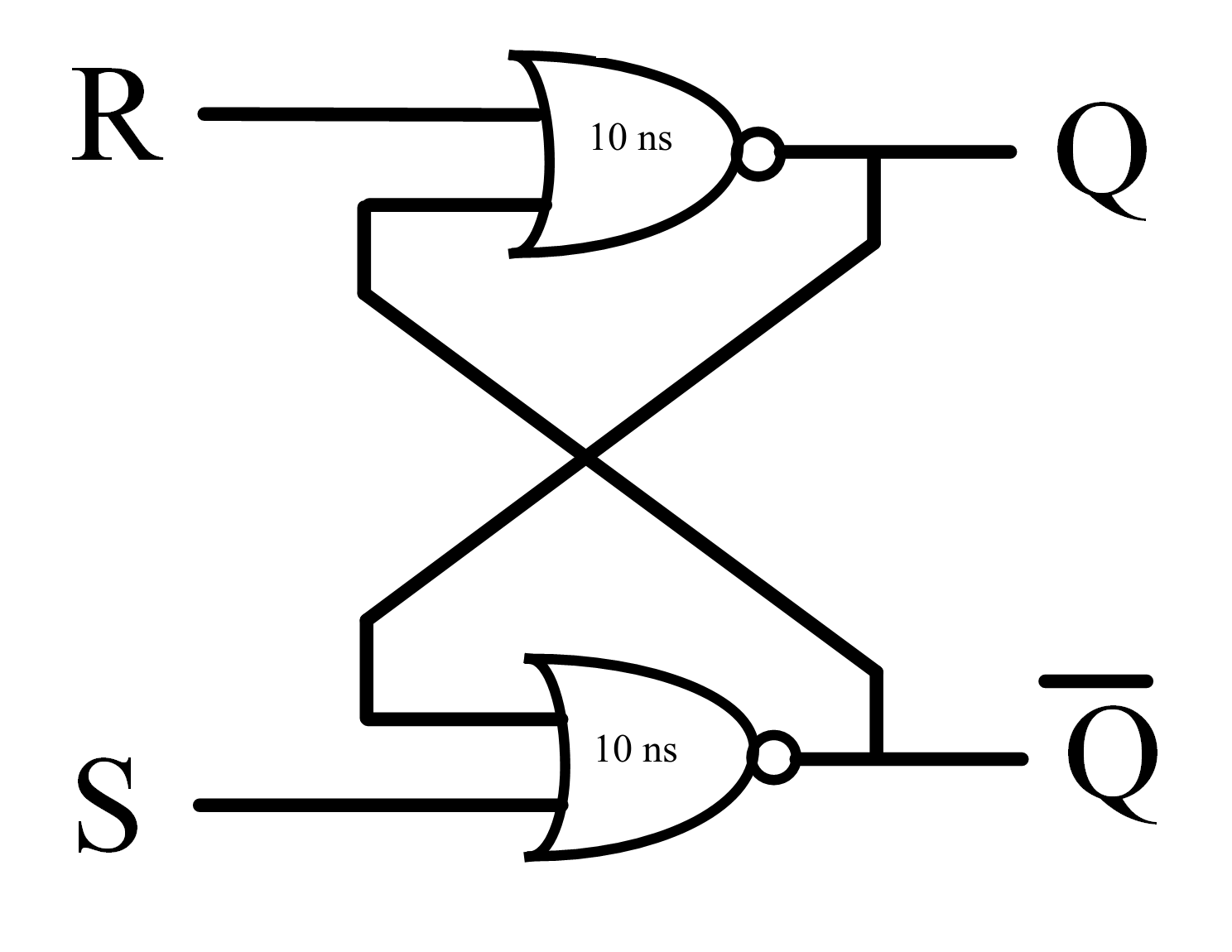
An SR-latch can be considered to be one-bit memory because it has two valid, stable states, which are affected by input pulses and persist even after the pulses. As you can be seen in the figure it has two inputs, and , and two complementary outputs, and .
The truth table of this circuit including inputs, output are given below.
| Inputs | Outputs | ||
|---|---|---|---|
| 0 | No Change | No Change | |
| 0 | 1 | 0 | 1 |
| 1 | 0 | 1 | 0 |
| 1 | 1 | Invalid | Invalid |
Based on the table, we can set and reset the output of the SR-latch, if {S,R} are {0,1},{1,0} respectively. If {S,R} is {1,1} the SR-latch operates as a memory and keep the value of its outputs.
The SR-latch discussed can be described using the following structural description:
`timescale 1ns / 1ps
module sr_latch(S, R, Q, Q_n);

	input logic S, R;
	output logic Q, Q_n;

	nor #10 i1(Q, R, Q_n);
	nor #10 i2(Q_n, S, Q);

endmodule
Note here that instead of using the naive unit delay, we model the NOR gates with delay 10 ns
The timescale directive at the top provides the default unit and the time resolution of the simulation
`timescale 1ns / 1ps
The following is a testbench for the SR-latch
`timescale 1ns / 1ps
module sr_latch_tb();

  logic S, R;
  logic Q, Q_n;

  // instantiate unit(module) under test
  sr_latch uut(.S(S), .R(R), .Q(Q), .Q_n(Q_n));

  initial
  begin
    $timeformat(-9,3," ns",20); //change the default display format for time
    $monitor("%10t: S=%b,R=%b,Q=%b,Q_n=%b", $time,S,R,Q,Q_n);
    $display("---------------------------------------------------------");
    S=1'b1; R=1'b0; // control input = set
    #1000 // wait 1000 ns
    $display("---------------------------------------------------------");
    S=1'b0; R=1'b0; // control input = hold
    #1000 // wait 1000 ns
    $display("---------------------------------------------------------");
    S=1'b0; R=1'b1; // control input = reset
    #1000 // wait 1000 ns
    $display("---------------------------------------------------------");
    S=1'b0; R=1'b0; // control input = hold
    #1000 // wait 1000 ns
    $display("---------------------------------------------------------");
    S=1'b1; R=1'b1; // control input invalid
    #1000 // wait 1000 ns
    $display("---------------------------------------------------------");
    S=1'b0; R=1'b0; // control input hold
    #1000 // wait 1000 ns
    $finish; // terminate the simulation
  end
endmodule
To compile using Icarus Verilog use the following commands at the command prompt:
iverilog -g2012 -o sr_latch_tb sr_latch.sv sr_latch_tb.sv
To run the simulation use the following command:
./sr_latch_tb
Here is a result found in the printed output:
---------------------------------------------------------
  0.000 ns: S=1,R=0,Q=x,Q_n=x
 10.000 ns: S=1,R=0,Q=x,Q_n=0
 20.000 ns: S=1,R=0,Q=1,Q_n=0
---------------------------------------------------------
1000.000 ns: S=0,R=0,Q=1,Q_n=0
---------------------------------------------------------
2000.000 ns: S=0,R=1,Q=1,Q_n=0
2010.000 ns: S=0,R=1,Q=0,Q_n=0
2020.000 ns: S=0,R=1,Q=0,Q_n=1
---------------------------------------------------------
3000.000 ns: S=0,R=0,Q=0,Q_n=1
---------------------------------------------------------
4000.000 ns: S=1,R=1,Q=0,Q_n=1
4010.000 ns: S=1,R=1,Q=0,Q_n=0
---------------------------------------------------------
5000.000 ns: S=0,R=0,Q=0,Q_n=0
5010.000 ns: S=0,R=0,Q=1,Q_n=1
5020.000 ns: S=0,R=0,Q=0,Q_n=0
5030.000 ns: S=0,R=0,Q=1,Q_n=1
5040.000 ns: S=0,R=0,Q=0,Q_n=0
5050.000 ns: S=0,R=0,Q=1,Q_n=1
5060.000 ns: S=0,R=0,Q=0,Q_n=0
5070.000 ns: S=0,R=0,Q=1,Q_n=1
5080.000 ns: S=0,R=0,Q=0,Q_n=0
5090.000 ns: S=0,R=0,Q=1,Q_n=1
5100.000 ns: S=0,R=0,Q=0,Q_n=0
5110.000 ns: S=0,R=0,Q=1,Q_n=1
5120.000 ns: S=0,R=0,Q=0,Q_n=0
5130.000 ns: S=0,R=0,Q=1,Q_n=1
...
← both Q and Q_n are low, this represents
an invalid output state
↓ oscillating (and invalid) output states
Note the invalid output pair Q=0,Q_n=0 on line 15 when S and R are both asserted.
Furthermore, on lines 17 onward note the problem that the simulator faces in computing a stable output when the invalid input is changed to 0,0. In fact this is not what happens in a real circuit. In a physical circuit, noise and positive feedback ensure that a stable state of 1,0 or 0,1 is reached. An analog circuit analysis is required to study how this happens. You may learn such analysis in later courses. This simulation result demonstrates that there are some limitations inherent to experiments with models based on digital abstractions of circuits.
Modeling analog circuits as digital circuits assumes certain rules will be followed. For a combinational circuit, the abstraction and modeling of the analog circuit as a digital circuit predicts behavior well as long as the inputs obey certain rules/constraints/requirements. Specifically, a minimum voltage threshold is specified for for a valid high input, and a maximum voltage threshold is specified for a valid low input. A sequential circuit also has timing requirements for the inputs (e.g. data, control, clock).
Prelab
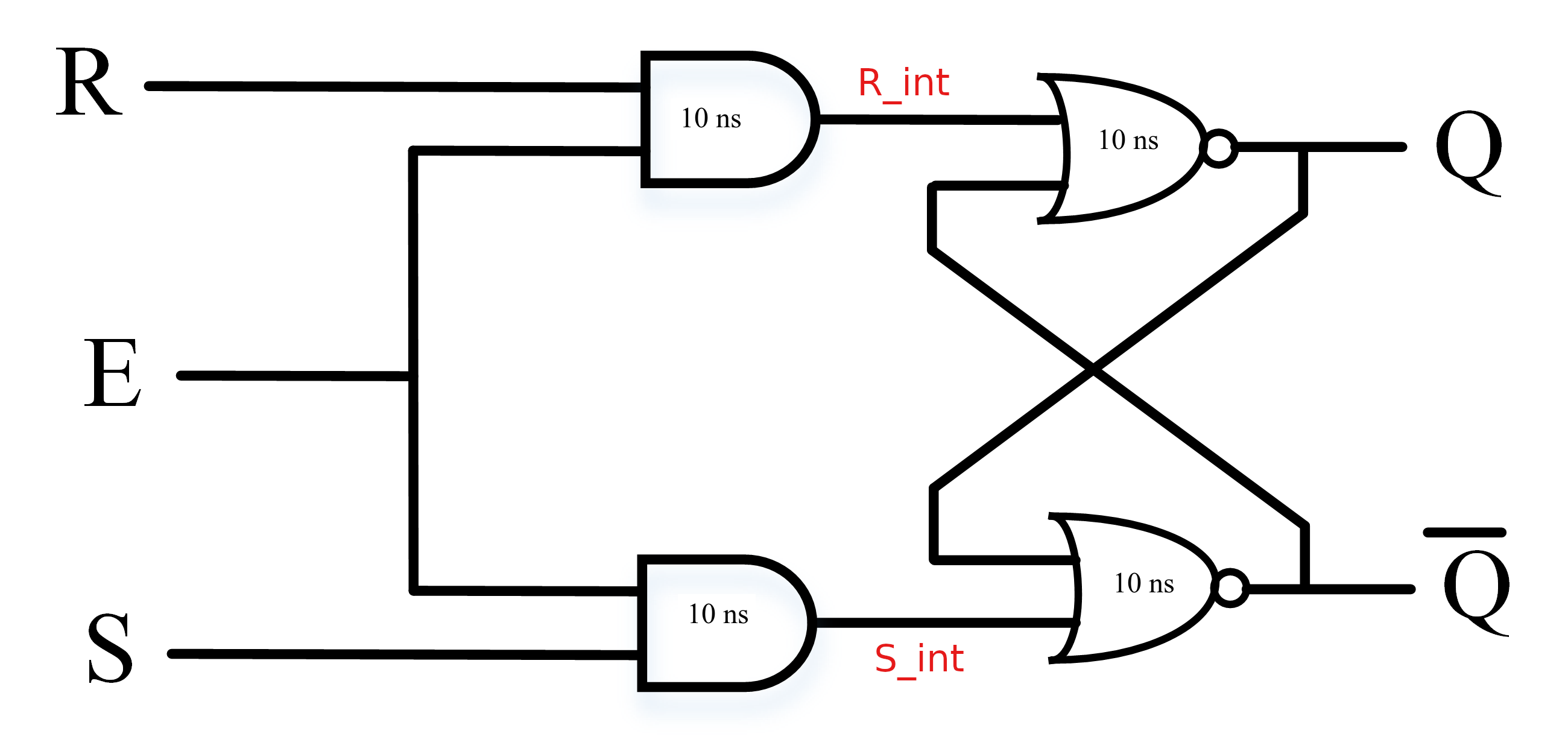
- Modify the provided Verilog for the SR latch to model a synchronous SR latch like the one to be build in the lab exercise.
- add a new input E to line 2 and 4 of the provided code.
- include the AND gates required using the verilog primative
and. Note that two new internal nets are required. Use thelogickeyword to define these. Assign a delay of “10 ns” to the AND gates using#10just as is for the NOR gates.
- Modify the provided testbench to include and control an enable signal. Explore all valid inputs and operations.
Take care to allow enabled operations (set/reset) to have sufficient time before enabling subsequent operations to avoid invalid behavior.
- Demonstrate the basic operation, noting any invalid behavior encountered and submit you code and results to the TA by the start of lab.
Lab Exercise
- Build a physical synchronous SR-Latch with enable using NOR and AND gates and show the valid operation. The circuit is shown in the following figure.
-
Complete the following truth table based on the synchronous SR-Latch circuit:
Input Output
StateNext Output
State1 0 0 0 ____ 1 ____ 1 0 0 ____ 1 ____ 0 1 0 ____ 1 ____ 1 1 0 ____ 1 ____ 0 0,1 0,1 0 ____ 1 ____
The following ICs are used in this lab:
Lab Report and Grading
- The prelab will be worth 20%
- Lab Exercise 60% (should be observable by the lab report and demonstration to the TA)
- Completion of the truth table demonstrated to the TA.
- Description of the obtained results in the lab report
- Lab Report (20%)
- Submit in the document the following (failure to submit may result in reduction of the Lab Exercise Grade)
- Verilog Code Listing for circuit modules if Separate from the Testbench
- Verilog Code Listing for Testbenche(s)
- Output listing (either from the screen waveform or from a file)
- Waveform plots are optional, but if provided key features should be easily visible and also annotated where possible
- be sure to discuss or note interesting results (don’t just dump the results and say “as can be seen it works”)
- Any the plots should be captioned. Mark axes with proper signal names. Tables should be properly titled, formatted, and captioned as well.
- Excessively long code or output listings that are not appropriate to include inline with the text should be moved the appendix, though key portions of the code and listing should be included in the text where possible a reference to the listing in the appendix.
- Comment and properly format the code that you include in the lab report.
- Testbenches should be included in the submission and must include the simulation control system task ‘$finish’, and be commented appropriately.
- Include a very brief discussion on what is shown in each plot or table.
- Describe the theory of operation of the circuits in your own words
- Specifically describe the difference of the synchronous and asynchronous operation
- Was the operation of the physical circuit consistent with the simulation? Note any differences observed.
- Submit in the document the following (failure to submit may result in reduction of the Lab Exercise Grade)