Lab 4: DeMorgans Theorem

Updated Fall 2021 Robucci
Updated Spring 2022 Robucci. Verilog pushed out of this lab for later to emphasis learning relation ships among switching functions, logic gates depicted in logic diagrams, and physical circuit components. IC depictions, symbols, and significant text modification. Expanded use of terms like boolean switching functions, logic diagrams, and circuit diagrams. Mentioned option for using a schematic-entry tool. Equipment and materials rewritten more clearly.
Table of Contents
Objective and Overview
In this labs students will learn to apply DeMogan’s Theorem to manipulate a logical expression and verify the operation, changing its mapping to digital logic gates. Students will work to develop their understanding of the relationship among Boolean switching functions, depictions in logic diagrams, and circuit diagrams and physical circuit implementations. In this lab, the physical circuit implementations are realized using 74LS series packaged gates. In this lab each physical IC has four logical gates, thus the use of Quad in the name of each, e.g. Quad 2-Input NAND, Quad 2-Input NOR, and Quad 2-Input AND. Students will exercise their ability to provide digital inputs using variants of the input generation and LED-based output indicator circuits used in previous labs.
Required Materials and Equipment
- One 74LS00: QUAD 2-input NAND gate https://www.futurlec.com/74LS/74LS00.shtml
- One 74LS32: QUAD 2-input OR gates https://www.futurlec.com/74LS/74LS32.shtml
- One 74LS08: QUAD 2-input AND gates https://www.futurlec.com/74LS/74LS08.shtml
- Two LEDs
- Three resistors
- Two resistors
- One breadboard
- One power supply (5V)
- One multi-meter
- One DIP switch package (has four switches)
Discussion and Theory
De Morgan’s Laws
A brief overview
De Morgan’s laws
In propositional logic and boolean algebra, De Morgan’s laws are a pair of transformation rules that are both valid rules of inference. These rules can be expressed as:
- the complement of the and of two signals is the same as the or of their complements:
- the complement of the or of two signals is the same as the and of their complements:
–quoted from https://en.wikipedia.org/wiki/De_Morgan’s_laws Wikipedia contributors. “De Morgan’s laws.” Wikipedia, The Free Encyclopedia. Wikipedia, The Free Encyclopedia, 9 Sep. 2021. Web. 22 Sep. 2021.
Example modifying circuit implementation of a switching function
In this example, a circuit having an and an gate will be analyzed and through manipulation of a switching function it will be redesigned using and gates.
The circuit suggested by the following logic diagram will be represented by a switching expression, which will then be manipulated so that a new alternative circuit can be built that has an equivalent functional model. The new circuit will be physically map to gates and a (a.k.a. an inverter).
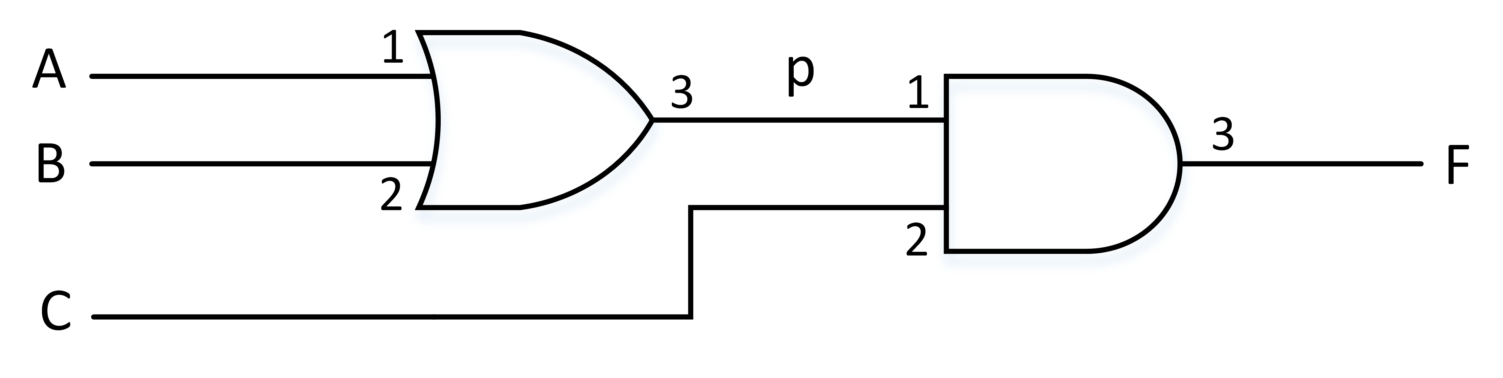
(pin numbers in this logic diagram correspond to pin numbers on your discrete 74LS ICs)
- The output of the circuit can be expressed as follows:
- If both sides of the equation are complemented, the equation sill holds:
This is not unlike multiplying both sides of an equation by -1 in traditional arithmetic. - Now, De Morgan’s law can be used on the right-hand side of the equation.
Note that though the original expression suggested that an gate would be used, the new expression requires no gates!
The only problem is that the expression is for , the complement of F, rather than F. - To obtain an expression for F, another complement of both sides of the equation can be applied:
the left-hand side of the equation is F complemented twice, which is just F.
As the equation shows, the function can be mapped to two gates as demonstrated in the following figure. The bubbles (tiny circles) on digital logic circuit symbols represent logical inversion.
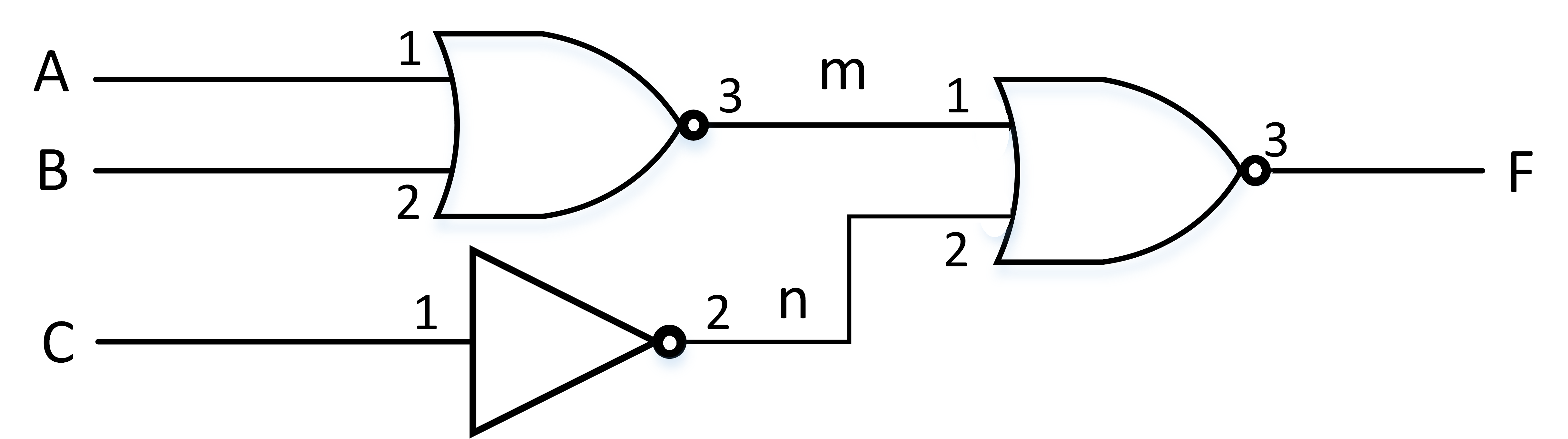
The truth table of this circuit including inputs, output, and intermediate signals are given below:
| Inputs | Intermediate Signals in Circuit 1 |
Intermediate Signals in Circuit 2 |
Output | |||
|---|---|---|---|---|---|---|
| A | B | C | p | m | n | F |
| L | L | L | L | H | H | L |
| L | L | H | L | H | L | L |
| L | H | L | H | L | H | L |
| L | H | H | H | L | L | H |
| H | L | L | H | L | H | L |
| H | L | H | H | L | L | H |
| H | H | L | H | L | H | L |
| H | H | H | H | L | L | H |
Prelab
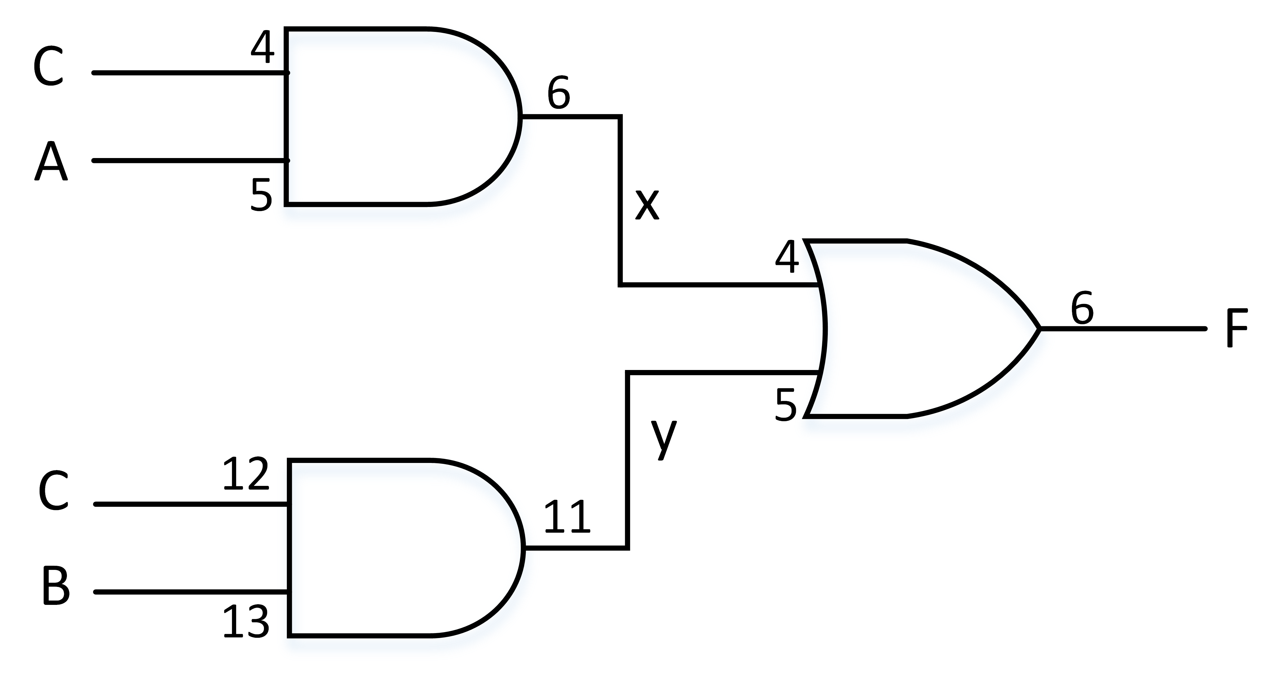
For the circuit represented by the following logic diagram, create an alternative implementation using DeMorgan’s Law, in the same manor as the example. Below you’ll need to complete the derivation of the alternate switching function and draw a logic diagram and finally depict the NAND-only version implemented of the circuit and complete the Truth Table for both implementations.
Packaged ICs
The ICs that will be used are depicted below. Each has four physical logic gates.

Initial Circuit Logic Diagram, with Physical Pin Annotations
The first circuit can be represented by the following logic diagram. Note that the power-supply connections are not represented. Additionally, the logic diagram has been annotated with pin numbers chosen from the physical packages.
Boolean Switching Function
-
Equation with Initial Expression
-
Complement both sides of the equation
= -
Apply De Morgan rule to the right-hand side
-
Complement both sides of the equation for the final Implementation (in this example comprises only NAND gates)
Alternate Logic Diagram, with Physical Pin Annotations
Finally, draw the logic diagram of the implementation with the only gates being gates.
In your diagram, label the output of the first gate and the output of the other gate
Additionally, annotate the inputs and output of the symbols with the physical pin numbers of the 74LS00 IC. This will aid contruction of the circuit. The datasheet is linked to in the Equipment and Materials Section for your convenience.
Truth Table
Lastly, fill in the following truth table for both implementations.
| Inputs | Output | Output | ||||||
|---|---|---|---|---|---|---|---|---|
| A | B | C | generated x | generated y | F (original circuit) |
generated u | generated v | F (alternate circuit) |
Pre-lab submission
Pre-lab submission
The steps of the derivation alternate boolean switching function, logic diagram and truth table shall comprise your pre-lab submission 📝.
Additional Preparation for the Lab (Circuit Diagram)
It would likely help to sketch a depiction of your circuit to aid planning and to reference as you build, debug, and demonstrate your circuit.
You can draw the circuit diagram using symbols like the following.

You can include input-generation circuits and LED output indicator circuits according if they may help you.
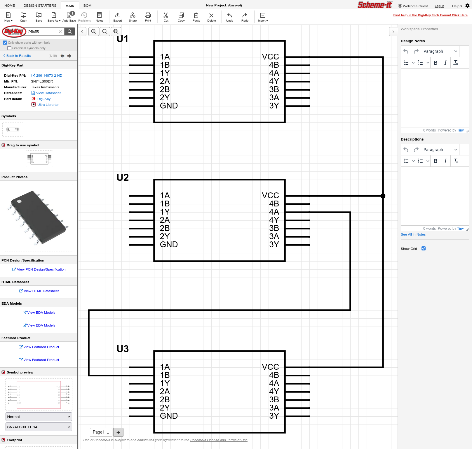
You can also use a schematic capture/ schematic entry tool to draw circuit diagrams. One such free online example is https://www.digikey.com/schemeit
Lab Exercise
Construct both circuits from the pre-lab, the one represented in the provided logic diagram and your design of the NAND-gate-only implementation. You must construct appropriate input-generation circuit and LED-based output indicators. These may be variants of the circuits used in previous labs.
📝 TA Verification
Have the TA check and record your completion.
Lab Report Submission
You should submit a brief technical written report as usual, but this time your report must include the following. The report in this lab is 10% of the lab grade.
You report should include the follow.
- Submit the logic diagrams and truth tables for both the circuits.
- The logic diagrams should be annotated with the physical pin numbers corresponding to the ICs that you used OR an additional circuit diagram depicting all physical pins, including VCC, GND, and unconnected pins on the IC packages used.
- A photograph of your constructed circuit. This is not a team lab. Every individual person must submit their own construction on the board that you signed out in the beginning of the semester.