Lab 3: Switching Expressions

Contributed to by Instructors Dr. Younis, Dr. Phatak, and dedicated TAs.
Updated Sept 15 2021 Robucci
Updated 2023-02 Robucci Added embedded applets, physical circuit drawings, changed schematic to match closely, improved pinout figures with indications of pin functions and enumerated embedded gates. Updated text to make reference to Boolean algebra rather than binary arithmetic. Updated procedure description to utilized detailed drawings rather than detailed text. Minor changes to gate and pin usage for more consistent order, though circuit is functionally the same. Debugging notes added.
Table of Contents
Objective and Overview
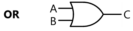
In this laboratory, students will learn to use physical and gates by implementing two equal logical expressions and verifying the equivalence (the same input values in both circuits should result in same output). Students will verify that , which can be shown analytically using the OR distributive law: .
To construct the circuits, students will use two ICs, a Quad 2-Input AND Gate IC and a Quad 2-Input OR Gate IC. DIP (dual inline packaged) switches and resistors will be used to provide inputs. LEDs and resistors will be used as output state indicators.
Required Equipment
- 74LS32: includes four 2-input OR gates https://www.futurlec.com/74LS/74LS32.shtml
- 74LS08: includes four 2-input AND gates https://www.futurlec.com/74LS/74LS08.shtml
- LEDs (x2)
- resistors (x2)
- breadboard
- power supply (5V)
- multi-meter
- DIP switch package (2x quad DIP switches)
- (Optional) 74LS11: 3-input AND Gate IC https://www.futurlec.com/74LS/74LS11.shtml
Discussion
In lecture, binary arithmetic and Boolean switching functions and Boolean algebra have been taught. It is important to understand how Boolean switching functions functions are implemented using logic gates so that you can learn to design your own physical implementations of logic functions. In is also important to understand how to use Boolean algebra to alter implementations of switching functions, which affects the circuits used to physically realize those functions. In this lab you will learn to build simple circuits from physical logic gates and test these circuits to verify functionally. You will verify that the distributive law of Boolean algebra can be used to construct two functionally equivalent circuits.
Digital Design of Complex Functions Using Logic Gates
Boolean logic gates can be used to implement complex operations. For example, in the image below a depiction of an 8-bit binary adder constructed from basic Boolean logic gates is shown.
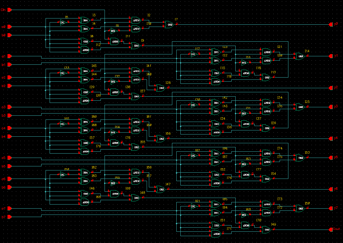
If you are comfortable with 8-bit binary addition, you can interact with the inputs in the embedded applet below and observe how Boolean logic gates can implement such an operation.
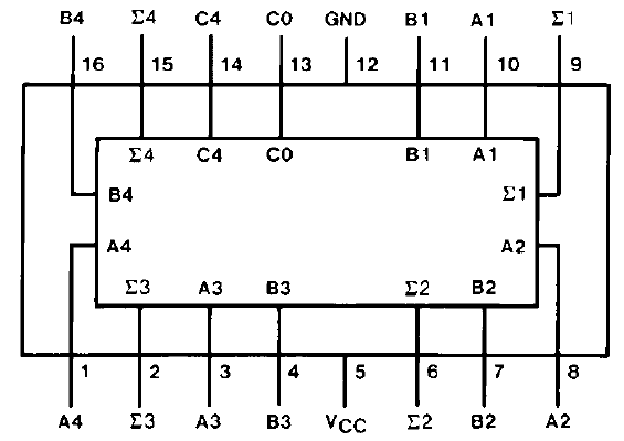
While it is reasonable to “breadboard” such a circuit, when one finds themselves in need of a common digital operation, such as addition, it is wise to see if an integrated circuit is available. For instance, a 4-bit adder is available as an integrated circuit, 74LS83: 4-bit Binary Full Adder.
Connection Diagram
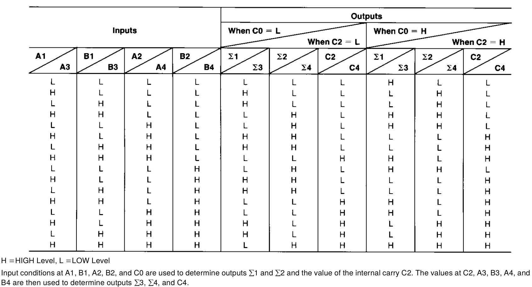
Truth Table
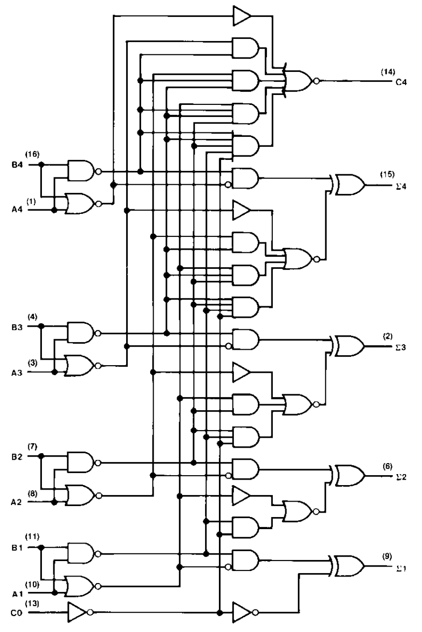
Logic Diagram
As you continue studies in digital design be sure to take note of and familiarize yourself with common circuits and functions, such as adders encoders, multiplexers, and shift registers. The family of 74LS series ICs is a good start. These types of common circuits are the building blocks of even more complex circuits. More complex circuits are now commonly implemented in single custom-designed ICs, VLSI (Very large Scale Integration), and Field-Programmable Gate Arrays (FPGAs), but the libraries for circuit implementations and the physical makeup of these devices are still commonly composed of (soon-to-be) familiar digital building blocks that you will learn in this course. Since they are common, work has been done to optimize their design and implementation — effort which you and other designers can leverage. In the case of breadboard implementation, one can also expect that an integrated circuit implementing an addition will be faster and use less power than a breadboard implementation of addition built from individual gates. However, to implement new custom circuitry and learn to build new digital building blocks in future technologies it is important for you to understand how to design with simple digital gates.
Manipulating and Mapping Boolean Functions towards Logic Gate Implementation
The following an example of the distributive law/property.
Using common Boolean algebra operators that are more convenient to type or write by hand, the equation may be shown analogously as follows
or written simply as
or
Common Boolean algebra operators are follows:
- denotes the single-bit OR operation, as in logical conjuction,
- denotes the single-bit AND operation, as in logical disjuction,
- denotes the single-bit NOT operation on , as in logical negation,
- denotes the XOR operation:
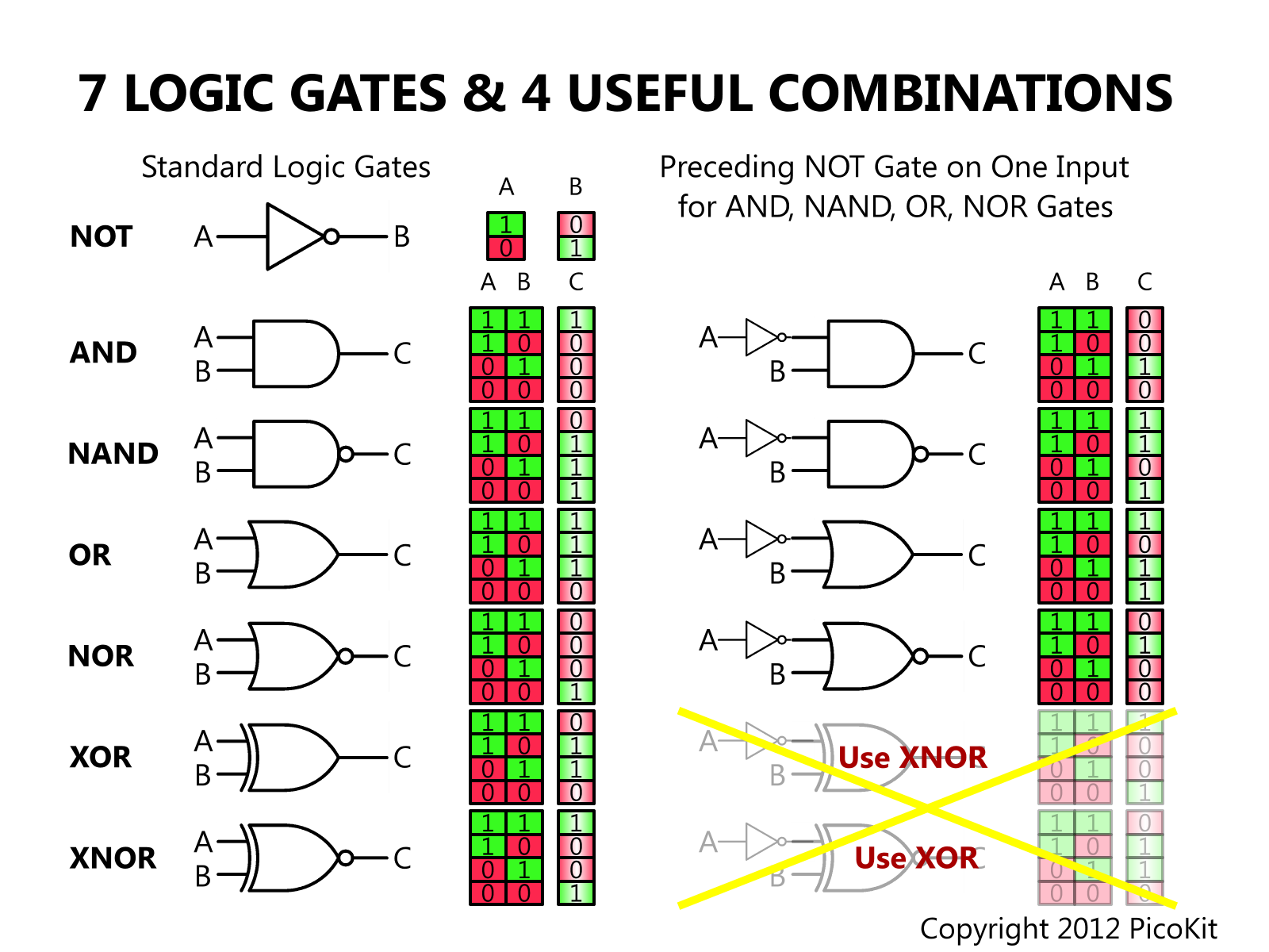
A Logic Gate is an idealized Boolean Function. It performs a logical operation on one or more inputs, producing a single output. Each kind of gate is associated with a distinctive shape/symbol, which is used for simple drawings and diagrams.
The following depicts other common logic gates, also sometimes called logic primatives.
By understanding the relationship of complex functions to truth tables and basic logic gates, one can learn to implement complex functions in physical circuits. By understanding the manipulation of these formulations, such as through Boolean algebra and various properties, one can find multiple possible implementations and learn to map a complex function to a desired set of building blocks or specific logic gates. Such a manipulation of a Boolean expression allows you to create of form that is directly mappable to available logic gates in a given technology. You can eventually learn to manipulate Boolean expressions to minimize size, area, or power of a circuits in later courses.
Lab Circuits
In particular, for this lab you will practice using logic gates by implementing the following Boolean operations:
Implementation 0
, which can be written as
Implementation 1
, which can be written as
In this lab, you will build these distinct functions, sharing only the inputs, and operating in parallel. The output of each circuit should be equivalent for all possible inputs state, meaning that the circuits are functionally equivalent.
The Pinouts for 7408 IC (AND gates) and 7432 IC (OR gates) are shown here:

You will only need to use three 2-input AND gates and two 2-input OR gates from these IC’s. Since the two expressions are 3-input functions, you will need to test 8 combinations of inputs.
Input circuit
The inputs will be generated the same as before. We will call the generated inputs A, B and C.

The orientation of switch DIP package and selection and order of switches used in the package may be different in the lab circuit.
(Optional) Alternative Input Circuit with Indicators
If you are comfortable building a more advanced input circuit, you can have LED input indicators.
Lower Logic-High Voltage
Be aware that this circuit will only generate around 3.35 V for input voltages. This is acceptable since the 74LS series ICs only requires 2.0 V for a valid high input voltage. However, you must be comfortable debugging this more advanced circuit (e.g. don’t expect 5 V at the inputs when measuring)

Extended Discussion
Though you wont be building an addition circuit in this lab, it is worth the insight at this point to understand how binary addition can be built from the logic gates like the ones you will use in this lab. You may appreciate how Boolean logic gates can be used to perform complex yet familiar computations.
Look closer at the way we do binary addition:
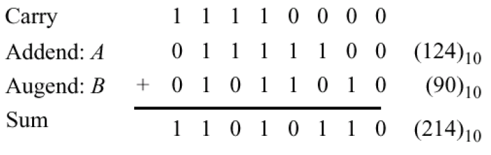
What we’re actually doing, can be described with Boolean logic and Boolean Algebra. For now, the discussion will be on one stage of addition. A give stage, indexed by i, has the following:
- three inputs: , and carry-in bit
- two outputs: the sum output result bit , and the carry-out bit to the next stage
The description in Boolean algebra is as follows:
- Expressions:
- , i.e. odd parity, an odd number of input bits are 1
- , i.e. at least two input bits are 1
Since we are able to describe binary addition with Boolean Logic, we are able to perform a single stage of the binary addition with logic gates:
Binary Full Adder:
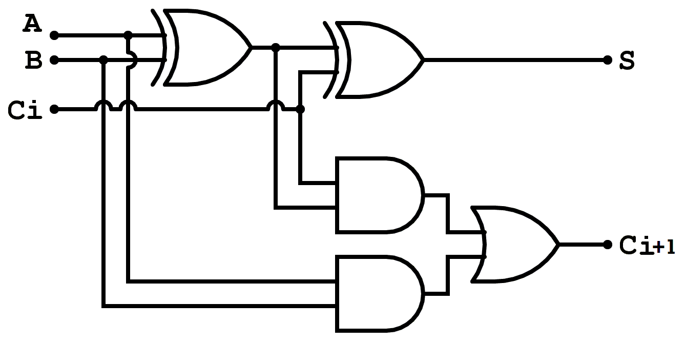
As an exercise in discussion session, we can verify that the truth table for these expressions matches the desired function for an addition.
Binary addition is not the only thing we can perform with logic gates. We can perform any kind of binary arithmetic with logic gates!
Here is an arithmetic logic unit (ALU) that can perform multiples type of basic operations:
Lab Reminders and Tips
- Keep power supply OFF until a circuit the is ready to be tested is fully connected and finished.
- If a circuit has two stages, such as in this lab, it is wise for a beginner to build the first stage and test it before building the second stage. You can test the output of the first stage using a multi-meter, avoiding the need to add LEDs to the intermediate circuit.
- Remember to turn power off while adding components or rewiring.
- A heating chip = wrong pin connection!!!
- Use colored wiring standard in your circuits where possible
- VCC = red
- GND = black/blue
Prelab
Using the started diagram below, sketch how you expect to position layout the ICs, resistors, LED and switch as well as what wire connections you would need to build the circuit show in the figure schematic in the Lab Procedure.

You may alternatively submit a photo of your breadboard with the components placed (though perhaps not yet wired).
Lab Procedure
Here is the depiction of final circuit to build and test in this lab:

The expected operation can be explored using the following embedded applet.
-
To begin construction, setup the three input-generation circuits and at least one active-high output indicator circuit with a resistor and LED.
-
Insert both ICs in the breadboard and connect GND and Vcc according to the pin assignment (in both of these ICs, pin# 7 is GND and pin# 14 is Vcc).
-
First, implement A(B+C) by making the appropriate connections.
- Add wires to connect the input-generating circuits to both 7408 and 7432
- Add additional wires to connect from the 7432 to the 7408
- From the 7408 to the output indicator circuit
-
Verify that the circuit is connected as follows and is working properly before adding additional wires.

Testing and Debugging — “We learn more from failure than success”
- Accept that you may have made a mistake. If you assume that you haven’t made a mistake you may bias your inspection. On the other hand, don’t assume that you have made a mistake either — the problem could be a broken wire. In any case, once the problem is found reflect and decide how you might reduce the chance of the problem in the future.
- Triple-checking every connection is a good idea, but use a multimeter (voltmeter) for debugging rather than repeatedly missing the same problem.
- Measure VCC and GND pins of each IC, with the negative probe of the multi-meter on the bench-top power supply’s negative terminal.
- It isn’t a bad idea in this lab to check the IC to see if the ICs are hot right after turning on the power supply. A hot IC indicates an over current situation, which can be caused by the presence of shorts between output or from outputs to a power supply source, mis-connected supply pins, or permanent damage from previous misusage.
- An extremely hot IC, especially if it remains so after output connections are removed, could indicate a “burned” IC.
- Measure each used input to the ICs, including any fixed inputs (non today). Voltages should be very close to VDD or GND. Change each input switch to verify. An invalid voltage could indicate an accidental short (two nodes connected that should not be or an accidental open (something not connected). (If you used the advanced input circuit with LED indicators, be aware that the generated voltage is around 3.35 V, but may be different depending on what LEDs you have in your kit)
- Measure the IC outputs under operation. Any invalid voltage could indicate a short or open.
- A regular, organized rather than haphazard layout of your circuit is easier to debug. The same goes for schematic capture (circuit drawing).
- At least to some degree, the flatter the the wires the better. Use the appropriate length for the job.
- Layout trial and error - it may be worth taking the time to re-build a circuit if a first layout approach leads to difficultly wiring neatly.
-
Once the first circuit is operational, implement AB+AC
- Add additional wires to connect the input generating circuits to the 7408.
- Add additional wires to connect the two 7408 outputs representing AB and AC to 7432
- Add additional wires to connect the appropriate 7432 output to the output indicator circuit
-
For all input combinations, compare the two FINAL outputs and ensure that they match. You can use the table below
Inputs Outputs A B C LED0 LED1 L L L _ _ L L H _ _ L H L _ _ _ _ _ _ _ _ _ _ _ _ _ _ _ _ _ _ _ _ _ _ _ _ _ _ _ -
📝 TA Verification
Have the TA check and record your completion. -
(Optional) Try to make a circuit for more complicated functions such as . The 74LS11 is triple 3-input AND gate.
Lab Report
You lab report should include an image of your completed circuit, the schematic redraw or copied, as well as the results that you obtained. Briefly explain each of these as you would to a fellow student just starting in the beginning of the semester. Be sure to clearly explain if you completed the work, or if some was not completed. Mention anything that didn’t work as expected and any incorrect results and comment appropriately mentioning your best explanation. Additional instructions may be posted on Blackboard.