Lab 2: Integrated Circuits and Binary Code Conversion
Previous Course Instructors Dr. Younis, Dr. Phatak
Updated by Dr. Robucci Sept 2021
Updated by Dr. Robucci Feb 2023 primarily adding more descriptions for digital circuit models, circuits, and including animations. Removed reference to wire colors.

Table of Contents
Objective and Overview
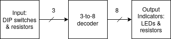
In this laboratory students will learn how to use a datasheet, an integrated circuit, and review the concept of binary codes by converting them to a decimal equivalent. The decimal equivalent is represented with a one-hot encoding, meaning one output is active at a time.
Students will use an IC, a 3-to-8 line decoder, as the basis of this lab. DIP (dual inline package) switches and resistors will be used to provide inputs. LEDs and resistors will be used as output state indicators.

Concepts and Theory
Integrated Circuit
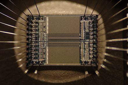
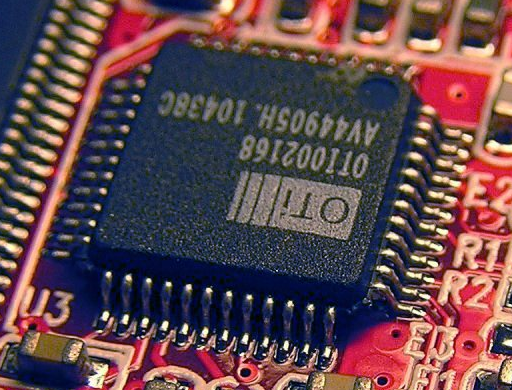
- An Integrated Circuit (also called chip) is an electronic circuit including thousands of millions small transistors, op-amps, capacitors, resistors, and etc. all located on a semiconductor wafer. In the image below, an IC is shown with bonding wires connected to it.
- These are also referred to as “chips,” or “microchips.”
- These can be Analog, Digital or Mixed Signal
- In the image below the IC can be seen through a window in a package.
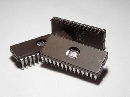
IC Packaging
The following are some common IC packages, which contain the IC, bonding wires and connections to physical pins, as well as mechanical body. The packaging also help dissipate heat away from the IC. Sometimes we say “chip” to referred to the package, and this is understood by the context of use.
- Through Hole:
- pins intended to go through a hole in a PCB board
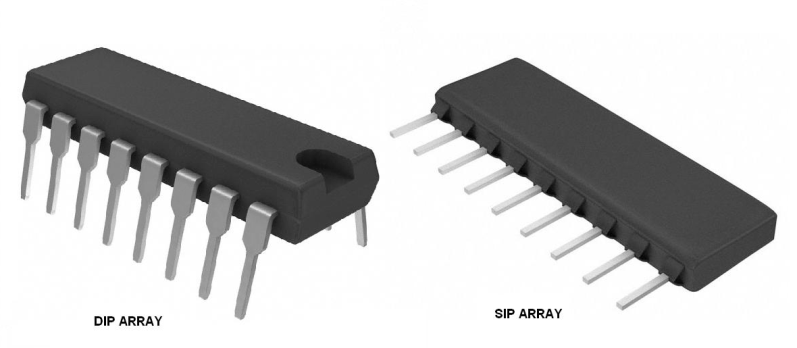
- Single In-Line Package (SIP)
- Dual In-line Package (DIP)
- https://en.wikipedia.org/wiki/Through-hole_technology
- pins intended to go through a hole in a PCB board
- Surface Mount
https://en.wikipedia.org/wiki/Surface-mount_technology - Flatpack (leads are cut to desired length)
https://en.wikipedia.org/wiki/Flatpack_(electronics)
May Other common types of packages exist, including Ball Grid Arrays (BGA) commonly used for microprocessors, though those types would not be used in this course.
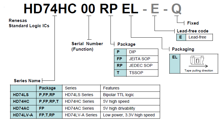
IC Part Numbering schemes
Number Schemes are used to identify parts, families of parts, and variants with different characteristics. The number schemes vary, so manufacture documentation must be examined.
Technical Datasheet
Technical Datasheet: a document containing the device’s technical characteristics including pin assignment, logic diagram, truth table, and operating details provided by the manufacturer.
- Datasheets for parts used in this course are openly available an indexed by web search engines. To find a datasheet use the following searchstring:
<Part Number> datasheet.- Example search:
74HC138AP datasheet
- Example search:
- Some key information found in datasheet:
- Pinout / Pin Assignment: provides mapping of physical pins to logic signals
- Logic Diagram: summary depiction (schematic) of underlying circuit
- Truth Table: table depicting function of combinational or sequential circuits
Pin Assignment / Pinout and Pin Numbering
“In electronics, a pinout (sometimes written “pin-out”) is a cross-reference between the contacts, or pins, of an electrical connector or electronic component, and their functions.” – “Pinout.” Wikipedia, Wikimedia Foundation, 2021-04-08, https://en.wikipedia.org/wiki/Pinout
Pin Assignments and Physical Pin Numbering
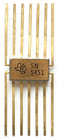
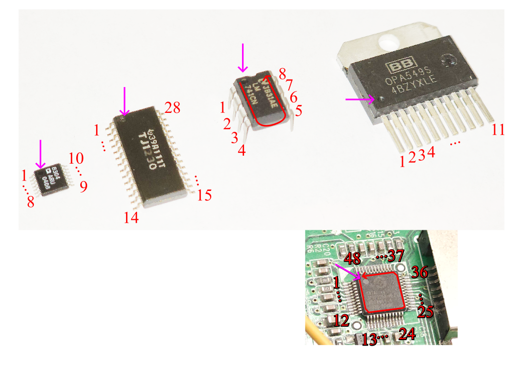
For dual-inline packages, the common convention is a pin numbering ordered physically in a counter-clockwise, or U-shape, starting with the #1 pin at the upper-left. The orientation of an IC is indicated by a marking on the package to uniquely identify pin 1. It is called a pin 1 indicator. Counter-clockwise numbering is common on other packages. Here is an image of various IC, with the pin 1 indicator pointed out as well as counter-clockwise numbering.
The datasheet will provide the mapping from physical pin numbers to pin names/labels/mnemonics. The pin names relate as meaningfully as possible to the function of the IC. The datasheet may refer to the mapping as pin assignment, pin configuration, etc… A diagram and/or a table will be provided.
Below is an example from a datasheet for an IC manufactured by Analog Devices.
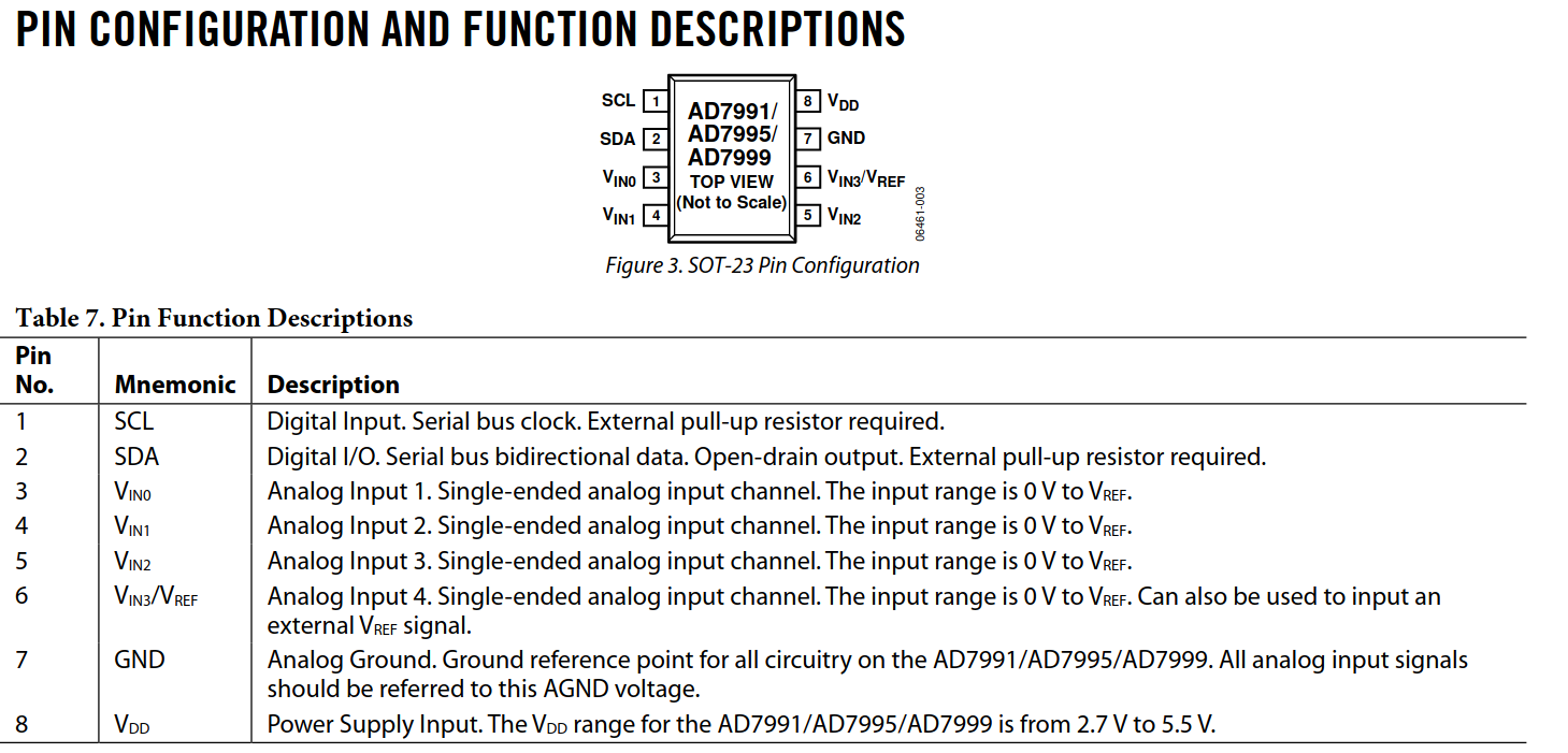
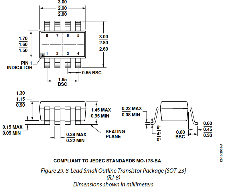
The pin-1 indicator is documented later in the datasheet in the physical drawing.
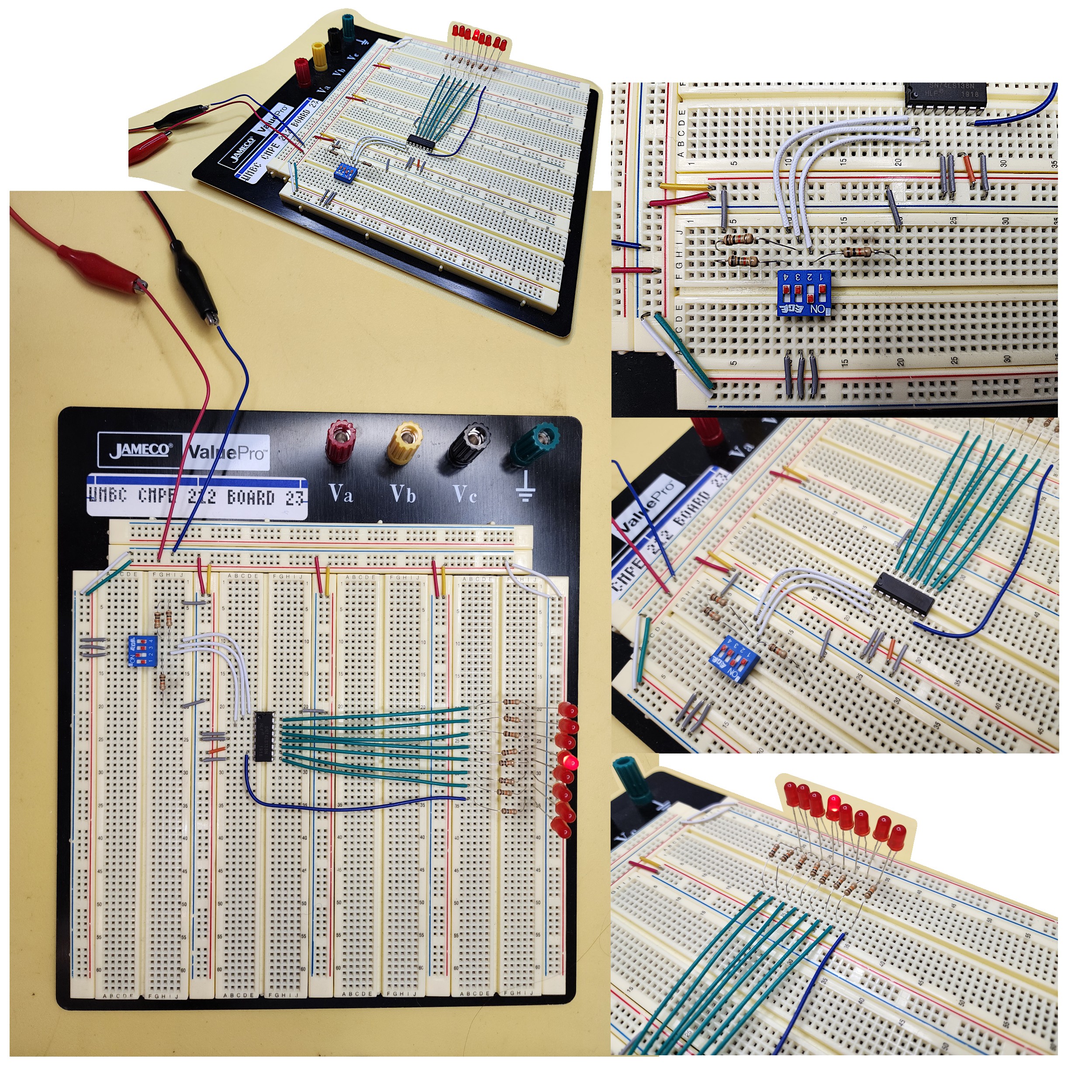
3-to-8 Decoder IC
The specific IC used in this lab decodes three binary weighted address inputs and controls eight mutually exclusive outputs – one of these outputs is active at a time. The outputs on this IC are active-low, meaning that the output is driven to a low voltage to indicate the active state. The current which drives the output low will be sourced from the power-supply through an LED to cause it to emit light. The IC has additional inputs other than the address pins that need to be set in order to see active outputs.
Link to datasheet: https://toshiba.semicon-storage.com/info/TC74HC138AP_datasheet_en_20140301.pdf?did=9405&prodName=TC74HC138AP
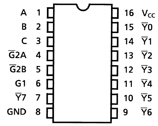
74HC138AP Pinout/Pin Assignment:
74HC138AP Truth Table:
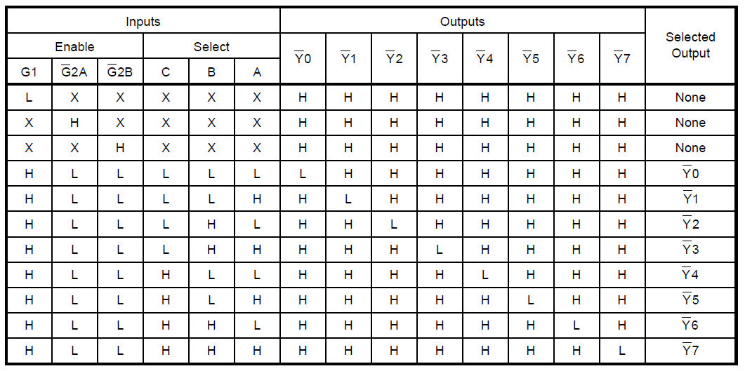
Voltage and Logic
-
We will use Voltage Logic Levels to assign logical values to the chip’s input pins.
-
In our circuit, the inputs are active high – small voltages (little difference in potential from GND) will serve as our logical 0, or “low” value, and VCC will be our logical 1, or “High” value.
-
Inputs A, B, and C can be set Low OR High, but the active-low outputs, Y, will change according to the truth table.
-
According to the truth table, and both need to be driven low, and G1 needs to be driven high to see outputs change according to the input address pins CBA
Breadboarding with DIP ICs
Dual inline packages with 100 mil center-to-center pin spacing (1 mil=1/1000th inch) can usually be placed in a breadboard straddling the center divider, connecting to terminal strips on either side of the divider. This placement provides multiple holes to electrically connect to each pin. Always be mindful of the PIN 1 INDICATOR. Use the power rails wherever possible to minimize the number of hookup wires that must be placed.

Tips for Beginners working with ICs
- Keep power supply OFF until circuit is finished.
- A heating chip = wrong pin connection!!!
- Where possible Use colored wiring standard in your circuits for power supply and meters
- VCC = red
- GND = black
- Use a multimeter to verify the operation of the input circuitry as well as the voltage at the pins labeled GND and Vcc . You would place the negative probe (black) lead on the ground net and the positive probe (red) lead on the net of interest to see the voltage. Values near 0 voltages considered 0 and values near 5 V are high. Values near the middle of the range might indicate a short or open in the circuit.
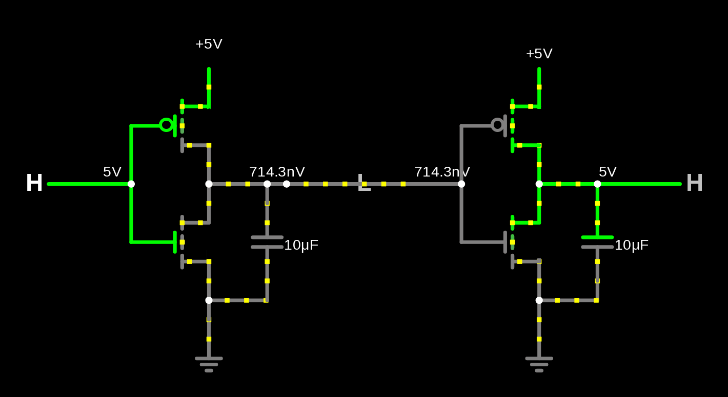
Physical Digital Circuits (Two-Inverter Discussion)
As you begin to work with physical circuits, you may benefit from an approximate mental model of how voltage is increased or decreased on a node when driven by a digital circuit. It is not expected understand this model, but its presentation to you may guide you as you develop an understanding or feeling of how the physical circuits work in relation to the functional descriptions that you will learn in class. In fact, fully understanding these components and circuits is a topic for a senior-level class. So don’t be discouraged if it doesn’t feel like this this model helps too much yet.
To gain a feeling of how a voltage may be set on a node by a digital circuit’s output driver, you can think of two switches called transistors connected to a capacitor in the configuration shown in the left half of the circuit below. The capacitor is like a battery that charges to a high voltage when current flows one way, and discharges to a low voltage when current flows the other way. Capacitance is a ratio-measure of the amount of charge required to change a voltage by a certain amount on such a component. Electrical current is the flow of charge. Even when not explicitly added as a component to a circuit, a implicit capacitance can be associated with a node (an implicit capacitance exist between you and earth ground for instance). Every node on your breadboard has a significant capacitance. You’ll learn more about capacitors and how to use them explicitly in later courses.
The transistors are of different types and are used differently. One transistor is connected to the high potential terminal of a power supply and when turned can supply current to charge the output node. The other transistor is used to draw current away from the output node to ground. The two transistors are different in that one is enabled by a low input voltage, and other other enabled by a high input voltage. As they are controlled, they can charge and discharge the capacitor.
This will be briefly demonstrated in simulation in-class. Each half of the circuit is an inverter, with the first output connected to the input of the second. Each invert implements the second simplest 1-bit digital function, the OUTPUT is the binary COMPLEMENT of the INPUT.When connected they form the simplest digital function, OUTPUT=INPUT.
Input Generation for this lab
-
Inputs A, B, and C will be driven using a DIP switch in combination with a pull-up resistor connected to Vcc.

-
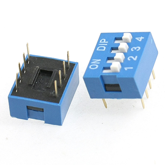
A DIP switch is a set of manual switches in a Dual In-line Package
-
A pull-up resistor is a resistor connected from a node to a high-potential supply node. Usually it provides for a “default” potential for a node, that may be readily over-driven by another component such as a switch that can short the node to ground.
-
-
Circuit Operation
-
If the switch is opened (disconnected/broken path), the resistor will pull the node to a high voltage via the resistor connected to Vcc.
-
When “closed” the switch “pulls” the free node between the resistor and switch to ground, so that the node exhibits a voltage representing logical ‘0’. Between the switch and the resistor, the switch wins in setting the node voltage since it has a higher conductance (lower resistance).
-
An implicit capacitor is depicted with dashed lines.

-
- In this lab, three switches are needed for three input-generating circuits.
- The part used in this lab contains four switches.
- Depiction of DIP switch used to build a circuit to control three node potentials:

Output Indicators
- You can use an Indicator Circuit built from an LED and current-limiting resistor.
- An LED is a light-emitting diode, which can be thought of as special “light” that must be connected with the correct polarity.
- A current-limiting resistor is a resistor placed in series with another component to reduce current flow that component.
- LED’s anode-cathode pins and how to connect them:
- The longer lead is typically the anode/positive connection
- The shorter lead typically the cathode/negative connection. The LED plastic assembly will also have a flat area as shown in the image below
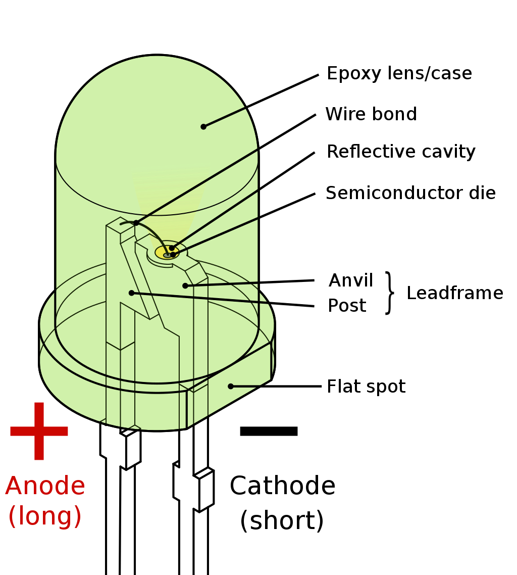

https://en.wikipedia.org/wiki/Light-emitting_diode
LED control with a Switch
A circuit such as the following can be used to control the current in an LED using a switch. When the switch allows current to flow, the LED may emit light. You are encouraged to build this circuit using a resistor and a switch if you have time. However, in this lab we’ll be interested in using a digital circuit to control the LED.

Active-High vs Active-Low Outputs
Standard digital circuit outputs can be thought of as a resistive switch that is connected to either drive the output to a high potential or to a low potential. Within each IC and each output, a driver circuit is responsible for driving the output node. The output driver state is controlled by other circuity within the same IC that implements a digital function. The state of the output driver may be active or inactive.
However, a port may be designated as type active-high or as type active-low.
The difference between active-high and active-low is which potentials (high vs. low) correspond to active and inactive. The tables below depict the difference for output drivers.
Active-High Output Driver Behavior:
| State 0=inactive 1=active | Active-High Output Driver Behavior |
|---|---|
| 0 | Tries to Drive Output to Low Potential |
| 1 | Tries to Drive Output to High Potential |
Active-Low Output Driver Behavior:
| State 0=inactive 1=active | Active-Low Output Driver Behavior |
|---|---|
| 0 | Tries to Drive Output to High Potential |
| 1 | Tries to Drive Output to Low Potential |
Appropriate LED-based Indicator Circuits for Active-High and Active-Low Outputs
An LED-based circuit may be used to monitor the electrical potential of a net (voltage with respect to common/ground), and therefore indirectly indicate the state of the output driver (if the circuit is operating correctly). An desirable configuration may be chosen depending on if one is monitoring an active-high output driver or an active-low output driver, such that the LED is ON when the output driver is in the ACTIVE state and the LED is OFF when the output driver is in the INACTIVE state.
LED-based Indicator Circuit for Active-High Output Driver

LED-based Indicator Circuit for Active-Low Output Driver

Active-High LED-based Indicators in Physical (Breadboard) Circuit
Shown in the next figure are three LED circuits with an active-high control input. The cathodes (as identified by the flat edges) are directed towards the lower potential ground, and the anodes (as indicated by the longer leads) are directed towards the input control. To limit the current and avoid burning the LED, a resistor can either be placed between the LED and ground, or between the control and the LED. In the figure the resistor is placed between the control input and the LED.
