Lab 10: Bidirectional Shift Register

Updated Nov 2021 Robucci
Updated 2023 April Robucci - minor textual updates, added red values to hold state depiction
Table of Contents
Objective
In this lab, students will verify the operation of a 4-bit bidirectional shift register, which features left shift and right shift capabilities, based on a D flip-flop (DFF), which is constructed using a JK flip-flop and an inverter.
- Bi-directional shift register
- shift register
- D flip-flop
- Construction of D flip-flop from a JK flip-flop and in input inverter
Required Equipment
- Dual JK Flip-Flop ('76 or '112 depending on part availability)
- 2x 7476/SN74LS76A: Dual JK Flip Flop with (Pre)set & Clear https://www.ti.com/lit/ds/symlink/sn5476.pdf or https://www.futurlec.com/74LS/74LS76.shtml
OR - 2x 74LS112 Dual Negative-Edge-Triggered Master-Slave J-K Flip-Flop
with Preset, Clear, and Complementary Outputs https://www.futurlec.com/74LS/74LS112.shtml
- 2x 7476/SN74LS76A: Dual JK Flip Flop with (Pre)set & Clear https://www.ti.com/lit/ds/symlink/sn5476.pdf or https://www.futurlec.com/74LS/74LS76.shtml
- 2x 74LS08: Quad 2-input AND
- 1x 74LS32: Quad 2-input OR
- 1x 74LS04: Hex Inverter
- 4x LEDs
- 1x Quad Switch
- 4x Resistor 330 Ω
- 3x Resistor 10 kΩ
Theory and Discussion
Flip-flops vs Latches with Enable
Latches with an enable signal have a mode to hold a signal, and another mode for which inputs propagate to the output. In the case of a D latch (e.g. SR-latch with and ) when the enable signal is asserted the output follows the input (with some delay) in a so-called transparent mode.
Flip-flops wait for a clock signal transition to propagate any single pending change to the output. There is no transparent mode.
JK Flip-Flop
The JK flip-flop has data inputs J and K with associated effects controlled by the signal clk. A 7476 JK flip-flop (or substitute part 74LS112) also has active low PRESET and CLEAR signals that bypass the clk control, and are thus called asynchronous inputs.

The function table show below is taken from http://www.ti.com/lit/ds/symlink/sn5476.pdf (substitute part 74LS112 is functionaly similar). Therein is used to represent the value of Q before the condition input condition described.
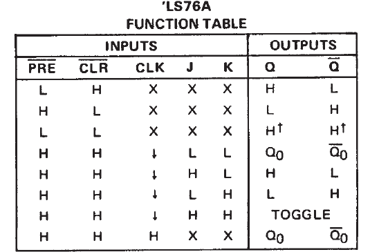
A reduced version without and can be considered, which can created using a SN74LS76A by tieing and to the power supply (high). The effective basic JK flip-flop circuit is shown below.

When the clock signal, , is low, the circuit is an a hold state, sustaining the output or using positive feedback, a loop of two inversions.

Otherwise, after the falling edge of the clock signal the output changes based on the inputs J and K inputs. The Setup time is the amount of time that J and K must be stable at the desired values while the clock signal is high before the falling edge of the clock signal in order to see consistent behavior as described in the function table.
In your simulations, be sure to change the input signal and let it be stable for sufficient time before the falling edge of the clock.
Provided Simulation Models
While Verilog provides built-in combinational primitives (e.g. not,nand,or), Verilog does not provide built-in sequential primitives. Therefore designers may utilize simulation models based on descriptive procedural code or user-defined primatives. Learning these is outside the scope of this course, so you will be provided a model to use in your design.
Minimal Functional Model using Behavioral Code
Here is one approach for a basic simulation model using procedural code. It could be suitable for functional simulation. You won’t use this model, but it may be of interest to some students for examination. Learning this style of procedural code modeling is outside the scope of this course.
//File: do not use this file
`timescale 1ns/1ps
module jk_ff_for_illustration (q,q_n,j,k,clk);
  output q;
  output q_n;
  input j;
  input k;
  input clk;
  parameter DELAY=1;
  logic q_int;

  initial q_int=0;

  assign #DELAY q=q_int;
  assign #DELAY q_n=~q_int;

  always @ (negedge clk)
    case ({j,k})
      2'b00:q_int<=q_int;
      2'b01:q_int<=0;
      2'b10:q_int<=1;
      2'b11:q_int<=~q_int;
      default:q_int<= 1'bx;
    endcase

error //this line is an intentional syntax error to dissuade use
endmodule
Provided UDP-Based Simulation Model for JK flip-flop
Here is the model that you will use for this lab. You will not be required to code a model like this for this course, but at least a cursory examination is useful. You may notice the definition of a Verilog user-defined primitive (UDP) using the keywords primitive and table. The model also includes a specify block to generate a clk-to-q timing delay of 20 ns. specify blocks are processed by Icarus Verilog when the -gspecifiy option is used and ignored otherwise.
//File: jk_ff.sv
`timescale 1ns/1ps
module jk_ff (q,q_n,j,k,clk,pre_n,clr_n);
   input j,k;
   output q,q_n;
   input  clk;
   input  pre_n,clr_n;

   logic  pre,clr;

   assign q_n=~q;
   assign pre=~pre_n;
   assign clr=~clr_n;
   jk_ff_prim i0 (q,j,k,clk,pre,clr);

   specify
      specparam Tsu=20;
      specparam Th=0;
      specparam Tco = 20;
      (clk => q) = Tco;          //enable 20 ns delay with -gspecify option
      $setup(negedge clk,j,Tsu); //not yet supported by icarus verilog
      $setup(negedge clk,k,Tsu); //not yet supported by icarus verilog
   endspecify

endmodule // jk_ff

primitive jk_ff_prim (q,j,k,clk,preset,clear);
   output q;
   input j,k,clk,preset,clear;

   reg   q;

   table
      //for UDP, only one edge is allowed per line
      //j k clk preset clear : old q : new q
      ? ? ? 1 0 : ?   :  1 ; //individual aync assertions
      ? ? ? 0 1 : ?   :  0 ;
      ? ? ? R ? : ?   :  - ; //ignore async rising edges
      ? ? ? ? R : ?   :  - ;

      ? ? ? F 0 : ?   :  - ; //ignore single-assertion falling edge
      ? ? ? 0 F : ?   :  - ;

      ? ? ? 1 1 : ?   :  0 ; //note that this is metastable and
                             // persistance after deasserting is
                             // not well-defined

      0 0 F 0 0 :  ?  :  -  ; //capture on falling edge of clk
      1 0 F 0 0 :  ?  :  1  ;
      0 1 F 0 0 :  ?  :  0  ;
      1 1 F 0 0 :  0  :  1  ;
      1 1 F 0 0 :  1  :  0  ;

      ? ? R 0 0 : ?   :  - ;   //ignore rising edge of clk
      * ? ? 0 0 : ?   :  - ;   // ignore edges on j
      ? * ? 0 0 : ?   :  - ;   // ignore edges on k


   endtable

endprimitive
The user-defined primative model also includes a specification of setup time violations, but unfortunately these are not implemented by Icarus Verilog at the time of this writing. If you perform the simulations on commercial simulations such as Cadence Xcelium (available via edaplayground.com ) warning can be generated. You will learn to use commercial simulators available at UMBC in later courses.
Here Example Warning Reported by Cadence Xcelium. This is not implemented in Icarus Verilog.
Warning!  Timing violation
           $setup( negedge clk:4 NS, j:5 NS,  20.000 : 20 NS );
            File: ./design.sv, line = 48
           Scope: test.dut
            Time: 5 NS
Here is a testbench that you can start with to verify your understanding of the operation of a JK Flip-Flop.
//File: jk_ff_tb.sv
`timescale 1ns/1ps
module jk_ff_tb;

   reg q,q_n,w1,w2;
   logic clk,j,k;

   logic pre_n;
   logic clr_n;


   jk_ff dut (q,q_n,j,k,clk,pre_n,clr_n);

   initial begin
      $display("j,k,clk,pre_n,clr_n,q,q_n,time");
      $monitor(j,k," ",clk," ",clr_n,pre_n," ",q,q_n,$time);
      j=0; k=0; clk=0; pre_n=1;clr_n=1;

      //fill in code here

      $finish;

   end


endmodule
To compile the design including the specify block, use the sepcify flag by including the option -gspecify. Additionally the option -Wall displays more warnings than the default.
The following generates the executable jk_ff_tb:
(the -Wall option prints more warnings which can help catch common mistakes)
iverilog -gspecify -Wall -g2012 jk_ff_tb.sv jk_ff.sv -o jk_ff_tb
Depending on the platform, you may need to run vvp or just the executable directly.
./jk_ff_tb
If your environment is not setup correctly, you may need to run this command instead:
vvp ./jk_ff_tb
New Setting: use specify blocks
Don’t neglect to provide the option -gspecify to iverilog. Otherwise the specify block in the provided model that provides the delay aspect of the model will be ignored.
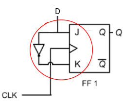
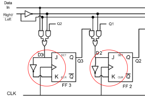
D flip-flop (DFF) constructed using a JK flip-flop
A JK flip-flop can be used to build a 1-bit data storage element by connecting J to an a data signal and K to an inverted version of the signal.
| J | K | |
|---|---|---|
| 0 | 0 | |
| 0 | 1 | 0 |
| 1 | 0 | 1 |
| 1 | 1 |
| input | intermediate | output | |
|---|---|---|---|
| D | J | K | |
| 0 | 0 | 1 | 0 |
| 1 | 1 | 0 | 1 |
Shift Register
The term register in digital logic can be used to generalize a collection of flip-flops used to store a digital word. Typically a register and word are distinguished by being associated with more than one bit, though a 1-bit register is conceptually valid.
In this lab you will make a shift register. A shift register is a cascade of flip-flops (can be any type; JK, D, T, etc…), where each flip-flop holds one bit of a binary number, and all of the flip-flops share the same clock signal. On every negative clock edge, the values held in the flip-flops will shift over to their neighboring flip-flops. The “Right/Left” wire determines which way they will shift. The value on the “Data In” wire is written to the empty flip-flop on the end.
Because this circuit allow
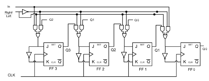
Here are some example behaviors, assuming that the stored binary number is denoted by Q[3,2,1,0].
- Right Shift
- If Q[3,2,1,0] == 0110, DataIn=0, R/L_n=1, the next value of Q[3,2,1,0] will be 0011.
- If Q[3,2,1,0] == 0110, DataIn=1, R/L_n=1, the next value of Q[3,2,1,0] will be 1011.
- Left Shift
- If Q[3,2,1,0] == 0110, DataIn=0, R/L_n=0, the next value of Q[3,2,1,0] will be 1100.
- If Q[3,2,1,0] == 0110, DataIn=1, R/L_n=0, the next value of Q[3,2,1,0] will be 1101.
Notice that we are wiring the K’s so that they are always the inverse of the J’s. When JK flip-flops are wired this way, they are synthesizing (or acting like) a D flip-flop.
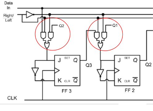
Next, notice how the combinational logic gates control the bit shifts.
With attention to the 2nd circle, observe that both Q3 and Q1 are fed into the AND gates.
If R/L_n = 0 (left shift), then Q1 is chosen to fill the F2 flip-flop.
If R/L_n = 1, then Q3 is chosen.
When a shift register can either shift left or right (ability to perform both operations), it’s called a bidirectional shift register.
Prelab
- Complete the testbench, jk_ff_tb.sv, demonstrating the behavior of the provided JK Flip-Flop. Perform the simulation and provide the results.
- Create a new module called d_ff, which uses the provided jf_ff and an inverter (inv) together to contruct a D Flip-Flop. Complete a new testbench d_ff_tb.sv demonstrating the behavior of the d_ff module. Perform the simulation and provide the results.
Lab Exercise
Build and demontrate the 4-bit bidirectional shift register.
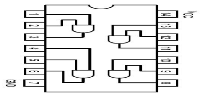
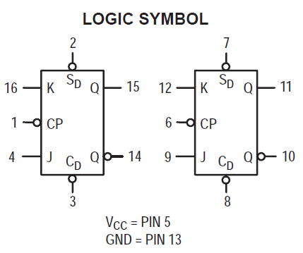
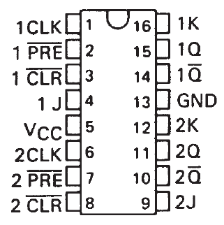
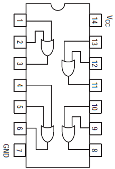
- For both the 74LS76 ICs, Pin# 2, 3, 5, 7, 8 have to be connected to Vcc and Pin #13 has to be connected to Ground. Note that the Vcc and GND pins are different from the normal ICs.
- Build the above circuit taking pin #15 and pin #11 of the first IC (7476) as Q0 and Q1, respectively and pin #15 and pin #11 of the second IC (7476) as Q2 and Q3, respectively.
- There are 3 inputs to the circuit, namely, DataIn, Right/Left_n (Direction), CLK. All of them should be connected to a switch.
- Pins #1 and #6 for both 74LS76 ICs should be connected to the CLK input.
- A single CLK pulse is triggered by changing from HI to LO (Since the FF is negative edge triggered). Make sure to bring the CLK to HI before triggering the second pulse.
- At every clock pulse triggered, the data will be shifted according to the Direction bit value. Refer to the following table for some examples.
- The shift register is set to 0000 by having DataIn set to 0 and giving 4 CLK pulses.
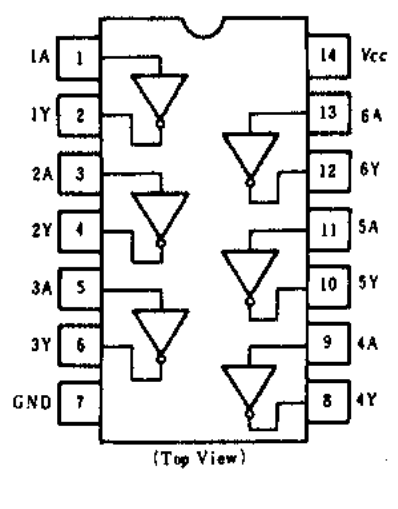
- See the Logic symbol and Pin diagram for the J and K inputs for the flip flops in the Appendix.
| CLK | Direction | DataIn | Data Out (Current) | Data Out (New) |
|---|---|---|---|---|
| LO–>HI | X | X | 1100 | 1100 |
| HI–>LO | 1 (Right) | 1 | 1100 | 1110 |
| HI–>LO | 1 (Right) | 0 | 1100 | 0110 |
| HI–>LO | 1 (Right) | 1 | 1010 | 1101 |
| HI–>LO | 1 (Right) | 0 | 1111 | 0111 |
| HI–>LO | 0 (Left) | 1 | 0110 | 1101 |
| HI–>LO | 0 (Left) | 0 | 1111 | 1110 |
| HI–>LO | 0 (Left) | 1 | 0000 | 0001 |
| HI–>LO | 0 (Left) | 0 | 1010 | 0100 |
Lab Report and Grading
- The prelab will be worth 20%
- Submit Verilog Code, including completed Testbench code, and simulation output results
- Lab Exercise 60%
- Lab Report 20%
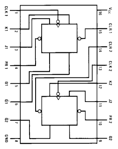
Appendix