Combinational Logic Design

Combinational Logic Design Vs. Sequential Logic

Combinational

Circuit gates interconnected by wires that carry logic signals are called combinational logic since the variables are combined by the logical operations. The output is based upon the input at the moment. Change the input, the output changes immediately. This makes it easy to use simple Boolean algebra as

Sequential

There are times when we need a different kind of logic. We needs circuits that can store information between operations and and use that remembered information to affect the next operation. That is called sequential logic

Combinational Design Concepts

A combinational circuit consists of input variables, output variables, gates, and connections. We can abstract a circuit into a block diagram.

As you can see there are some number (n) of inputs and some number (m) of outputs. What happens in the block can be described using a truth table where each input is given with the resulting output for that set of inputs. It takes m expressions, one for each output.

Requirements Specification

As in software, we have a requirements specification of some form. Assume we have a 9-Input odd function, showing if we have an odd number of 1's in the input. One solution is to break it down into a set 3-Input odd functions that their result is feed into another 3-Input odd function. We can break that down into two XOR gates. Each XOR can then be broken down into a set of NANDs. This results in the following chart:

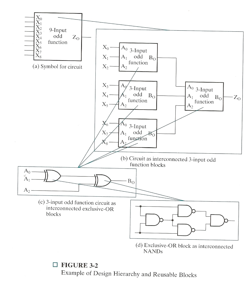
Logic and Computer Design Fundamentals, 3rd Ed., Mano and Kime, Prentice Hall, 2004, Page 90

Another way to diagram this is:

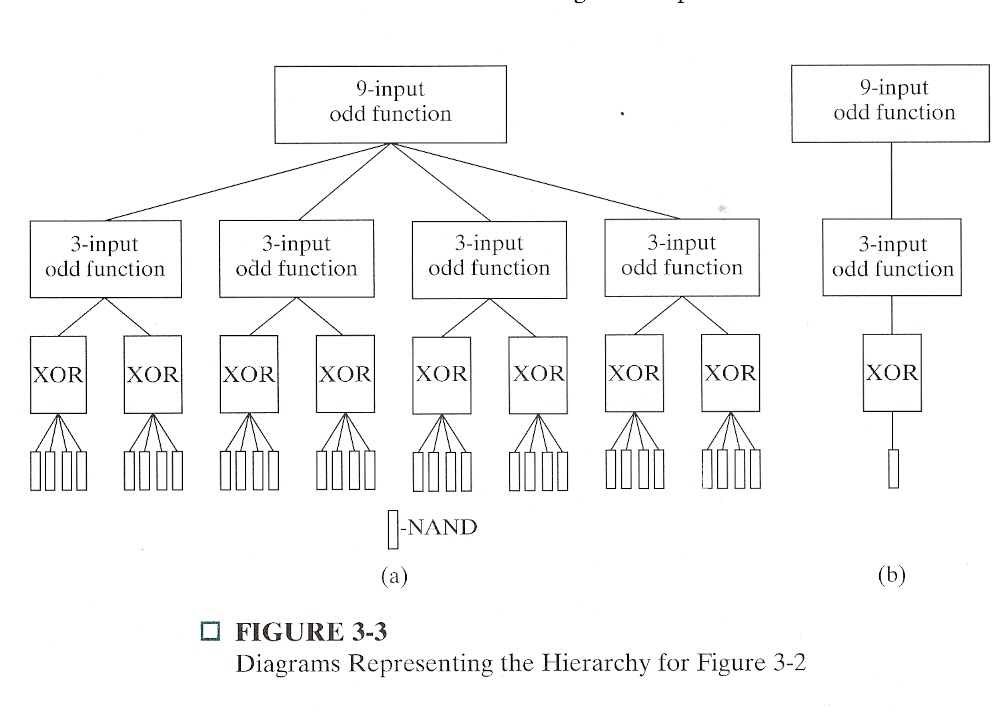
Logic and Computer Design Fundamentals, 3rd Ed., Mano and Kime, Prentice Hall, 2004, Page 91

As you can see, the principles of top-down design and functional decomposition apply to hardware as well as software. The other software principle here is reuse, by instantiating a good design again and again.

Complexity

As projects get bigger and bigger, involving more circuits, the design gets more complex. To hand the complexity, there are computer-assisted design (CAD) tools. The Hardware Description Languages (HDL) provide those tools, such libraries, logic simulator, and logic synthesizers. The two best known are VDHL and Verilog.

Technology Parameters

Fan-in
The maximum number of inputs allowed to be available on a gate.
Fan-out
The maximum number of gates that can be driven by the output.
Cost
The measure of a gate's contribution to the cost of the IC.
Propagation delay
The time that is required for a change in value of a signal to go from input to output of a gate.
Power dissipation
The power consumed is dissipated as heat.

Voltage

The voltage is often describe as 0 and 1. However, when the voltage changes, it takes time for the voltage to go from low to high. It is not instantaneous. It takes a tiny amount of time to rise or fall. Also, the voltage can be slightly lower or higher than specified. It is normal to have a range for 0 and another range for 1. There is a range in the middle where things are not defined. For example, 0.0 to 0.2 could be considered 0, 0.8 to 1.0 could be considered 1 and the range of greater that 0.2 and less than 0.8 is the undefined transitional state.

Propagation Delay

The propagation delay is the delay from one reference voltage to the other. It is possible that the delay for changing from 0 to 1 known as low-to-high propagation time (tPLH) is not the same as changing from 1 to 0 high-to-low propagation time (tPHL), so the propagations delay (tpd) is the largest of the two values.

Fan-out

A way to measure the output from a gate is by the number of gates can use that output as input. The term for driving one gate is one standard load. If we have a gate that has an output of 4 standard loads, then it can drive four other gates.

As an example, suppose we have an AND gate with a standard load of 6 but we need to drive 8 other gates. What we can do is amplify the signal with a buffer. In this case the buffer must have a standard load of at least 3. That would look like this:

Positive And Negative Logic

Normally, the two output values are H and L, where H is 1 and L is 0. This is called positive-logic. There are times when designs prefer to have H as 0 and L as 1. This is called negative-logic.

Design Procedure

Just as there is in designing software, there is a methodology in hardware design:

Specification
If it does not exist, then a specification must be written in either text or a Hardware Description Language (HDL). This must include all of the inputs and outputs.
Formulation
This is the truth table or Boolean equations that expresses the output based on the input.
Optimization
This uses the all the techniques to produce the circuit with the lowest cost.
Technology mapping
Express the optimized circuit using the appropriate implementation technology, full custom design, standard cell design, or gate array.
Verification
Prove the correctness of the final design, manually or with simulation.

Example -- BCD to Excess-3 Converter

The excess-3 code for a decimal digit is the binary combination for the corresponding decimal digit plus 3, such that 6 is 6 + 3 or 9 in excess-3 code. BCD is a method for encode number values in four bits, so you can encode two decimal digits per byte.

Specification

Each BCD digit is four bits labeled A, B, C, and D, where A is the most significant bit. Each excess-3 digit is 4 bits labeled W, X, Y, and Z, where W is the most significant. This converter will change the BCD code input and output the corresponding excess-3 code.

Formulation

The following is the truth table for the converter.

Decimal DigitBCD Input Excess-3 Output
ABCD WXYZ
0 0000  0011
1 0001  0100
2 0010  0101
3 0011  0110
4 0100  0111
5 0101  1000
6 0110  1001
7 0111  1010
8 1000  1011
9 1001  1100
10 1010  XXXX
11 1011  XXXX
12 1100  XXXX
13 1101  XXXX
14 1110  XXXX
15 1111  XXXX

NOTE:The last six input values are don't-care conditions because they are not possible and that have no output.

Optimization Using K-maps

We have to compute each of the excess-3 bits independently of each other. To calculate W, we use a K-map and put a one into each square for each one in the truth table (m5 - m9). Then we put an X into m10 - m15. Next we optimize. Then we do the other three bits: X, Y, and Z.

Results


© 2007 Gary L. Burt