<- previous index next ->
The "cache" is very high speed memory on the CPU chip.
Typical CPU's can get words out of the cache every clock.
In order to be as fast as the logic on the CPU, the cache
can not be as large as the main memory. Typical cache sizes
are hundreds of kilobytes to a few megabytes.
There is typically a level 1 instruction cache, a level 1
data cache. These would be in the blocks on our project
schematic labeled instruction memory and data memory.
Then, there is typically a level 2 unified cache that is
larger and may be slower than the level 1 caches. Unified
means it is used for both instructions and data.
Some computers have a level 3 cache that is larger and
slower than the level 2 cache. Multi core computers
have at least a L1 instruction cache and a L1 data cache
for every core. Some have a L3 unified cache that is
available to all cores. Thus data can go from one core
to another without going through RAM.
+-----------+ +-----------+
| L1 Icache | | L1 Dcache |
+-----------+ +-----------+
| |
+---------------------------+
| L2 unified cache |
+---------------------------+
|
+------+
| RAM |
+------+
|
+------+
| Disc | or Solid State Drive, SSD
+------+
The goal of the architecture is to use the cache for instructions
and data in order to execute instructions as fast as possible.
Typical RAM requires 5 to 10 clocks to get an instruction or
data word. A typical CPU does prefetching and branch prediction
to bring instructions into the cache in order to minimize
stalls waiting for instructions. You will simulate a cache and
the associated stalls in part 3 of your project.
Intel IA-64 cache structure, page 3
IA-64 Itanium
An approximate hierarchy is:
size response
CPU 0.5 ns 2 GHz clock
L1 cache .032MB 0.5 ns one for instructions, another for data
L2 cache 4MB 1.0 ns
RAM 4000MB 4.0 ns
disk 500000MB 4.0 ms = 4,000,000 ns
A program is loaded from disk, into RAM, then as needed
into L2 cache, then as needed into L1 cache, then as needed
into the CPU pipelines.
1) The CPU initiates the request by sending the L1 cache an address.
If the L1 cache has the value at that address, the value is quickly
sent to the CPU.
2) If the L1 cache does not have the value, the address is passed to
the L2 cache. If the L2 cache has the value, the value is quickly
passed to the L1 cache. The L1 cache passes the value to the CPU.
3) If the L2 cache does not have the value at the address, the
address is passed to a memory controller that must access RAM
in order to get the value. The value passes from RAM, through
the memory controller to the L2 cache then to the L1 cache then
to the CPU.
This may seem tedious yet each level is optimized to provide good
performance for the total system. One reason the system is fast is
because of wide data paths. The RAM data path may be 128-bits or
256-bits wide. This wide data path may continue through the
L2 cache and L1 cache. The cache is organized in blocks
(lines or entries may be used in place of the word blocks)
that provide for many bytes of data to be accessed in parallel.
When reading from a cache, it is like combinational logic, it
is not clocked. When writing into a cache it must write on
a clock edge.
A cache receives an address, a computer address, a binary number.
The parts of the cache are all powers of two. The basic unit of
an address is a byte. For our study, four bytes, one word, will
always be fetched from the cache. When working the homework
problems be sure to read the problem carefully to determine if
the addresses given are byte addresses or word addresses.
It will be easiest and less error prone if all addresses are
converted to binary for working the homework.
The basic elements of a cache are:
A valid bit: This is a 1 if values are in the cache block
A tag field: This is the upper part of the address for
the values in the cache block.
Cache block: The values that may be instructions or data
In order to understand a simple cache, follow the sequence of word
addresses presented to the following cache.
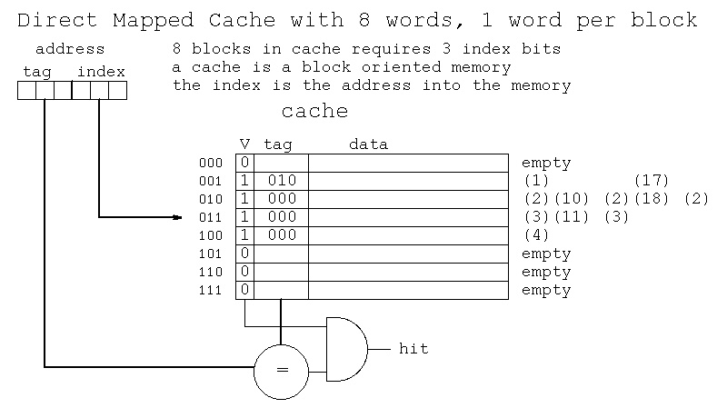 Sequence of addresses and cache actions
decimal binary hit/miss action
tag index
1 000 001 miss set valid, load data
2 000 010 miss set valid, load data
3 000 011 miss set valid, load data
4 000 100 miss set valid, load data
10 001 010 miss wrong tag, load data
11 001 011 miss wrong tag, load data
1 000 001 hit no action
2 000 010 miss wrong tag, load data
3 000 011 miss wrong tag, load data
17 010 001 miss wrong tag, load data
18 010 010 miss wrong tag, load data
2 000 010 miss wrong tag, load data
3 000 011 hit no action
4 000 100 hit no action
Sequence of addresses and cache actions
decimal binary hit/miss action
tag index
1 000 001 miss set valid, load data
2 000 010 miss set valid, load data
3 000 011 miss set valid, load data
4 000 100 miss set valid, load data
10 001 010 miss wrong tag, load data
11 001 011 miss wrong tag, load data
1 000 001 hit no action
2 000 010 miss wrong tag, load data
3 000 011 miss wrong tag, load data
17 010 001 miss wrong tag, load data
18 010 010 miss wrong tag, load data
2 000 010 miss wrong tag, load data
3 000 011 hit no action
4 000 100 hit no action
 Sequence of addresses and cache actions
decimal binary hit/miss action
tag index word
1 00 00 01 miss set valid, load data (0)(1)(2)(3)
2 00 00 10 hit no action
3 00 00 11 hit no action
4 00 01 00 miss set valid, load data (4)(5)(6)(7)
10 00 10 10 miss set valid, load data (8)(9)(10)(11)
11 00 10 11 hit no action
1 00 00 01 hit no action
2 00 00 10 hit no action
3 00 00 11 hit no action
17 01 00 01 miss wrong tag, load data (16)(17)(18)(19)
18 01 00 10 hit no action
2 00 00 10 miss wrong tag, load data (0)(1)(2)(3)
3 00 00 11 hit no action
4 00 01 00 hit no action
There are many cache organizations. The ones you should know are:
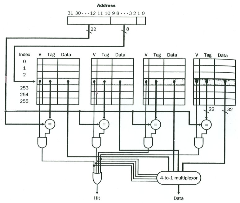
A direct mapped cache: the important feature is one tag comparator.
An associative cache: the important feature is more than one tag
comparator. "Two way associative" means two
tag comparators. "Four way associative means
four tag comparators.
A fully associative cache: Every tag slot has its own comparator.
This is expensive, typically used for TLB's.
For each organization the words per block may be some power of 2.
For each organization the number of blocks may be some power of 2.
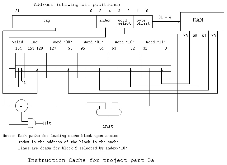
The size of the address that the cache must accept is determined by
the CPU. Note that the address is partitioned starting with the
low order bits. Given a byte address, the bottom two bits do
not go to the cache. The next bits determine the word. If there
are 4 words per block, 2-bits are needed, if there are 8 words per
block, 3-bits are needed, if there are 16 words per block 4-bits
are needed. 2^4=16 or number of bits is log base 2 of number of words.
The next bits are called the index and basically address a block.
For 2^n blocks, n bits are needed. The top bits, whatever is not
in the byte, word or index are the tag bits.
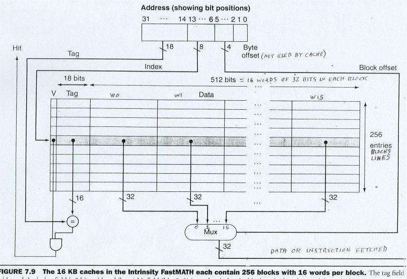
Given a 32-bit byte address, 8 words per block, 4096 blocks you would
have: byte 2-bits
word 3-bits
index 12-bits
tag 15-bits
---- +-----+-------+------+------+
total 32-bits | tag | index | word | byte | address
+-----+-------+------+------+
15 12 3 2
To compute the number of bits in this cache:
4096 x 8 words at 32 bits per word = 1,048,576
4096 x 15 bits tags = 61,440
4096 x 1 bits valid bits = 4,096
----------
total bits = 1,114,112 (may not be a power 0f 2)
Each cache block or line or entry, for this example has:
valid tag 8 words data or instructions
+-+ +----+ +----------------------------+
|1| | 15 | | 8*32=256 bits | total 272 bits
+-+ +----+ +----------------------------+
then 12 bit index means 2^12=4096 blocks. 4096 * 272 = 1,114,112 bits.
Cache misses may be categorized by the reason for the miss:
Compulsory miss: The first time a word is used and the block that
contains that word has never been used.
Capacity miss: A miss that would have been a hit if the cache was big enough.
Conflict miss: A miss that would have been a hit in a fully associative cache.
The "miss penalty" is the time or number of clocks that are required to
get the data value.
Data caches have two possible architectures in addition to all
other variations. Consider the case where the CPU is writing
data to RAM, our store word instruction. The data actually is
written into the L1 data cache by the CPU. There are now
two possibilities:
Write back cache: the word is written to the cache. No memory access
is made until the block where the word is written
is needed, at which time the entire block is
written to RAM. It is possible the word could be
written, and read, many times before any memory access.
Write through cache: the word is written to the cache and the single
word is sent to the RAM memory. This causes to
RAM memory to be accessed on every store word but
there is no block write when the block is needed
for other data. Most of the memory bandwidth
is wasted on a wide 128 or 256 bit memory bus.
Tradeoff: Some motherboards have a jumper that you can change to
have a write back or write through cache. My choice is
a write back cache because I find it gives my job mix
better performance.
16 words per block. Note partition of address bits.
Sequence of addresses and cache actions
decimal binary hit/miss action
tag index word
1 00 00 01 miss set valid, load data (0)(1)(2)(3)
2 00 00 10 hit no action
3 00 00 11 hit no action
4 00 01 00 miss set valid, load data (4)(5)(6)(7)
10 00 10 10 miss set valid, load data (8)(9)(10)(11)
11 00 10 11 hit no action
1 00 00 01 hit no action
2 00 00 10 hit no action
3 00 00 11 hit no action
17 01 00 01 miss wrong tag, load data (16)(17)(18)(19)
18 01 00 10 hit no action
2 00 00 10 miss wrong tag, load data (0)(1)(2)(3)
3 00 00 11 hit no action
4 00 01 00 hit no action
There are many cache organizations. The ones you should know are:
A direct mapped cache: the important feature is one tag comparator.
An associative cache: the important feature is more than one tag
comparator. "Two way associative" means two
tag comparators. "Four way associative means
four tag comparators.
A fully associative cache: Every tag slot has its own comparator.
This is expensive, typically used for TLB's.
For each organization the words per block may be some power of 2.
For each organization the number of blocks may be some power of 2.
The size of the address that the cache must accept is determined by
the CPU. Note that the address is partitioned starting with the
low order bits. Given a byte address, the bottom two bits do
not go to the cache. The next bits determine the word. If there
are 4 words per block, 2-bits are needed, if there are 8 words per
block, 3-bits are needed, if there are 16 words per block 4-bits
are needed. 2^4=16 or number of bits is log base 2 of number of words.
The next bits are called the index and basically address a block.
For 2^n blocks, n bits are needed. The top bits, whatever is not
in the byte, word or index are the tag bits.
Given a 32-bit byte address, 8 words per block, 4096 blocks you would
have: byte 2-bits
word 3-bits
index 12-bits
tag 15-bits
---- +-----+-------+------+------+
total 32-bits | tag | index | word | byte | address
+-----+-------+------+------+
15 12 3 2
To compute the number of bits in this cache:
4096 x 8 words at 32 bits per word = 1,048,576
4096 x 15 bits tags = 61,440
4096 x 1 bits valid bits = 4,096
----------
total bits = 1,114,112 (may not be a power 0f 2)
Each cache block or line or entry, for this example has:
valid tag 8 words data or instructions
+-+ +----+ +----------------------------+
|1| | 15 | | 8*32=256 bits | total 272 bits
+-+ +----+ +----------------------------+
then 12 bit index means 2^12=4096 blocks. 4096 * 272 = 1,114,112 bits.
Cache misses may be categorized by the reason for the miss:
Compulsory miss: The first time a word is used and the block that
contains that word has never been used.
Capacity miss: A miss that would have been a hit if the cache was big enough.
Conflict miss: A miss that would have been a hit in a fully associative cache.
The "miss penalty" is the time or number of clocks that are required to
get the data value.
Data caches have two possible architectures in addition to all
other variations. Consider the case where the CPU is writing
data to RAM, our store word instruction. The data actually is
written into the L1 data cache by the CPU. There are now
two possibilities:
Write back cache: the word is written to the cache. No memory access
is made until the block where the word is written
is needed, at which time the entire block is
written to RAM. It is possible the word could be
written, and read, many times before any memory access.
Write through cache: the word is written to the cache and the single
word is sent to the RAM memory. This causes to
RAM memory to be accessed on every store word but
there is no block write when the block is needed
for other data. Most of the memory bandwidth
is wasted on a wide 128 or 256 bit memory bus.
Tradeoff: Some motherboards have a jumper that you can change to
have a write back or write through cache. My choice is
a write back cache because I find it gives my job mix
better performance.
16 words per block. Note partition of address bits.
 A four way associative cache. Note four comparators.
Each of the four caches could be any of the above architectures
and sizes.
A four way associative cache. Note four comparators.
Each of the four caches could be any of the above architectures
and sizes.
 Homework 9 on cache
The motherboard is essential to support the CPU, RAM and
other devices.
Battle of the MotherBoards
An Asus motherboard example
Asus motherboards
2007 Mother Boards, note RAM and hard drive capability
Graphics Cards for mother boards without enough power
Latest high speed IBM Power6, 448 cores at 4.7Ghz
Water cooled
Homework 9 on cache
The motherboard is essential to support the CPU, RAM and
other devices.
Battle of the MotherBoards
An Asus motherboard example
Asus motherboards
2007 Mother Boards, note RAM and hard drive capability
Graphics Cards for mother boards without enough power
Latest high speed IBM Power6, 448 cores at 4.7Ghz
Water cooled
<- previous index next ->