<- previous index next ->
We now start the second half of the semester, focusing on
the five part project to simulate part of a real computer.
Note that the hardware does not change. Only multiplexer
control signals are needed to execute various instructions.
The first complete computer architecture is a single cycle design.
On each clock cycle this computer executes one instruction. CPI=1
(The clock would be slow compared to pipeline computers in the
next lecture.)
Signals are inputs to components on the left and outputs of
components on the right. Wide lines are 32-bits. Narrow signals
are one-bit unless otherwise indicated.
 Every clock, we use the rising edge, the program counter register, PC,
takes the 32 bit input from the left most signal on the diagram. The
output of the PC is a memory address for an instruction.
The 32 bit instruction is "decoded" by routing various parts of the
instruction to various places.
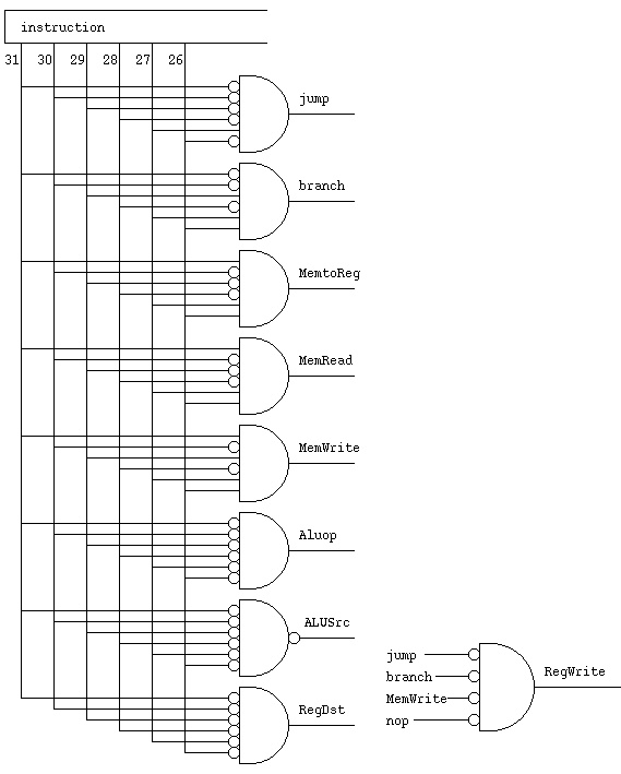
Bits 31 downto 26 of the instruction go to the control unit.
(The schematic of the control unit is shown below.)
Bits 10 downto 0 of the instruction go to the ALU, the shift count and
the ALU op code.
Bits 25 downto 21 are a register address that is read and the 32 bit
contents of that register are placed on read data 1.
Bits 20 downto 16 are a register address that is read and the 32 bit
contents of that register are placed on read data 2.
Bits 15 downto 11 are a register address that may be written with the
32 bit write data.
Bits 25 downto 0 go to the jump address computation.
The sequence of diagrams that follow will show the control signals
and the data paths for various instructions.
The bit patterns for our CMSC 411 machine are cs411_opcodes.txt
inside the ALU entity
The first instruction is the nop instruction.
This instruction shows the basic updating of the PC, while changing
no other registers or memory. All other instructions shown below,
except branch and jump , use this updating of the PC.
Every clock, we use the rising edge, the program counter register, PC,
takes the 32 bit input from the left most signal on the diagram. The
output of the PC is a memory address for an instruction.
The 32 bit instruction is "decoded" by routing various parts of the
instruction to various places.
Bits 31 downto 26 of the instruction go to the control unit.
(The schematic of the control unit is shown below.)
Bits 10 downto 0 of the instruction go to the ALU, the shift count and
the ALU op code.
Bits 25 downto 21 are a register address that is read and the 32 bit
contents of that register are placed on read data 1.
Bits 20 downto 16 are a register address that is read and the 32 bit
contents of that register are placed on read data 2.
Bits 15 downto 11 are a register address that may be written with the
32 bit write data.
Bits 25 downto 0 go to the jump address computation.
The sequence of diagrams that follow will show the control signals
and the data paths for various instructions.
The bit patterns for our CMSC 411 machine are cs411_opcodes.txt
inside the ALU entity
The first instruction is the nop instruction.
This instruction shows the basic updating of the PC, while changing
no other registers or memory. All other instructions shown below,
except branch and jump , use this updating of the PC.
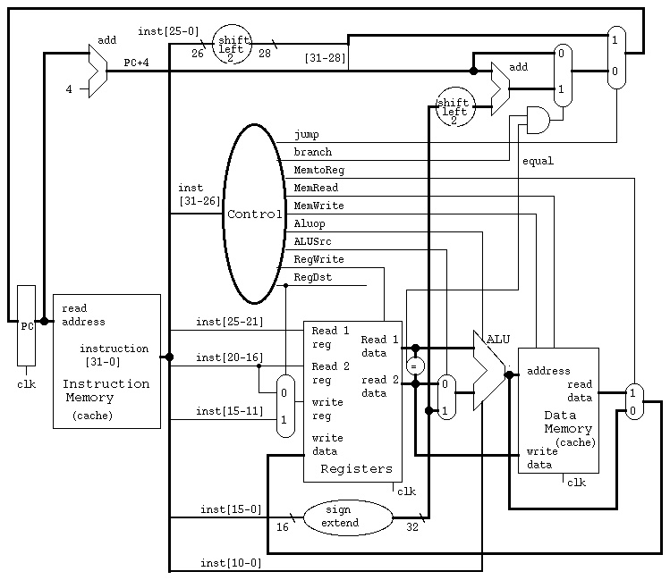
nop
 The PC plus 4 is the next sequential instruction address. The 32 bit
instruction has four bytes. The bottom two bits of all instruction
addresses are zero. The instructions are "aligned."
The critical control signals are:
jump 0
branch 0
MemWrite 0
RegWrite 0
The other control signals are shown for completeness.
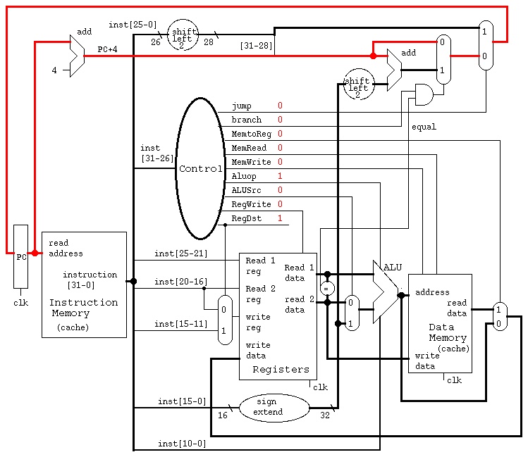
The next instruction, jump, is just slightly more complex than nop.
The bit pattern for jump in cs411_opcodes.txt
The PC plus 4 is the next sequential instruction address. The 32 bit
instruction has four bytes. The bottom two bits of all instruction
addresses are zero. The instructions are "aligned."
The critical control signals are:
jump 0
branch 0
MemWrite 0
RegWrite 0
The other control signals are shown for completeness.
The next instruction, jump, is just slightly more complex than nop.
The bit pattern for jump in cs411_opcodes.txt
jump
 Note the wiring where instruction bits 25 downto 0 are shifter left
two places. This provides a larger jump range and aligns the address
on a quad byte boundary. The top four bits come from the incremented PC
and the resulting 32 bit address is routed through the multiplexer back
to the PC, ready for the next clock.
The critical control signals are:
jump 1
MemWrite 0
RegWrite 0
The other control signals are shown for completeness.
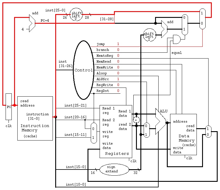
The next instruction, branch , uses the remainder of the upper
schematic to compute a new instruction address relative to the
incremented PC. Note that the assembler subtracts 4 from the
branch address before generating the machine instruction.
The bit pattern for beq in cs411_opcodes.txt
Note the wiring where instruction bits 25 downto 0 are shifter left
two places. This provides a larger jump range and aligns the address
on a quad byte boundary. The top four bits come from the incremented PC
and the resulting 32 bit address is routed through the multiplexer back
to the PC, ready for the next clock.
The critical control signals are:
jump 1
MemWrite 0
RegWrite 0
The other control signals are shown for completeness.
The next instruction, branch , uses the remainder of the upper
schematic to compute a new instruction address relative to the
incremented PC. Note that the assembler subtracts 4 from the
branch address before generating the machine instruction.
The bit pattern for beq in cs411_opcodes.txt
branch
 Note the equal comparator immediately next to the registers.
This is the design we will use in the project because it provides
better performance in the pipeline architecture.
If the branch condition is not satisfied, the instruction becomes
a nop . The branch condition for beq is that the contents of
the registers are the same and a beq instruction is executing.
Note the and gate driving the multiplexer.
The critical control signals are:
jump 0
branch 1 and the equal comparison
MemWrite 0
RegWrite 0
The other control signals are shown for completeness.
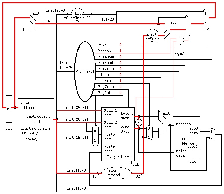
The add instruction is shown with just the data paths and
control paths for the instruction shown. The upper control to
increment the PC is the same as shown for the nop instruction.
The bit pattern for add in cs411_opcodes.txt
Note the equal comparator immediately next to the registers.
This is the design we will use in the project because it provides
better performance in the pipeline architecture.
If the branch condition is not satisfied, the instruction becomes
a nop . The branch condition for beq is that the contents of
the registers are the same and a beq instruction is executing.
Note the and gate driving the multiplexer.
The critical control signals are:
jump 0
branch 1 and the equal comparison
MemWrite 0
RegWrite 0
The other control signals are shown for completeness.
The add instruction is shown with just the data paths and
control paths for the instruction shown. The upper control to
increment the PC is the same as shown for the nop instruction.
The bit pattern for add in cs411_opcodes.txt
add
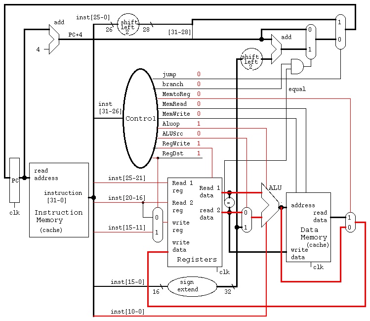 The contents of two registers are combined in the ALU. The ALU op
code in the instruction bits 5 downto 0 would have 100000 for add .
Other instructions such as subtract, shift, and, etc follow the
same data paths and control, executing the instruction coded in
the instruction bits 5 downto 0. The output of the ALU is routed back
to the registers and written on the falling edge of the clock, clk.
The critical control signals are:
jump 0
branch 0
MemtoReg 0
MemWrite 0
Aluop 1
ALUSrc 0
RegWrite 1
RegDst 1
The other control signals are shown for completeness.
The load word, lw , instruction computes a memory address using
the twos complement offset in the instruction bits 15 downto 0,
sign extended to 32 bits and added to a register. The memory is
read and the contents from memory is routed through the multiplexer
into the destination register. The PC is incremented as shown in
the nop instruction.
The bit pattern for lw in cs411_opcodes.txt
The contents of two registers are combined in the ALU. The ALU op
code in the instruction bits 5 downto 0 would have 100000 for add .
Other instructions such as subtract, shift, and, etc follow the
same data paths and control, executing the instruction coded in
the instruction bits 5 downto 0. The output of the ALU is routed back
to the registers and written on the falling edge of the clock, clk.
The critical control signals are:
jump 0
branch 0
MemtoReg 0
MemWrite 0
Aluop 1
ALUSrc 0
RegWrite 1
RegDst 1
The other control signals are shown for completeness.
The load word, lw , instruction computes a memory address using
the twos complement offset in the instruction bits 15 downto 0,
sign extended to 32 bits and added to a register. The memory is
read and the contents from memory is routed through the multiplexer
into the destination register. The PC is incremented as shown in
the nop instruction.
The bit pattern for lw in cs411_opcodes.txt
load word, lw
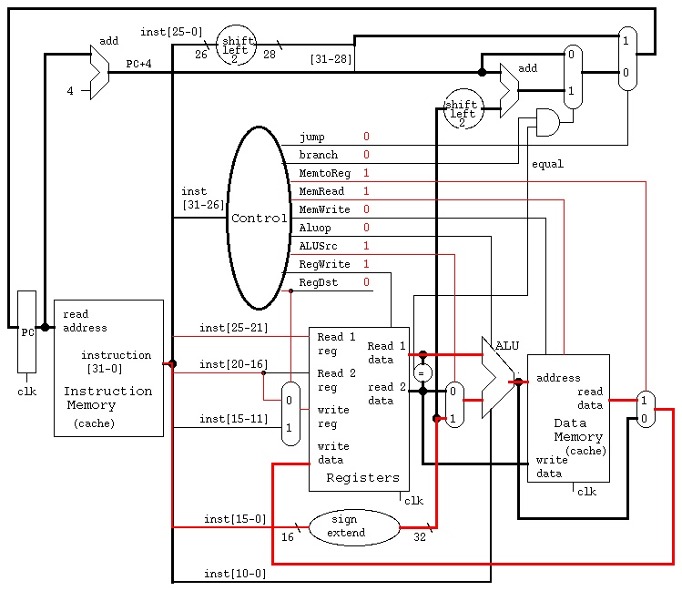 The critical control signals are:
jump 0
branch 0
MemtoReg 1
MemRead 1
MemWrite 0
Aluop 0 the ALU performs an add when Aluop is zero
ALUSrc 1
RegWrite 1
RegDst 0
The other control signals are shown for completeness.
The store word, sw , instruction computes a memory address using
the twos complement offset in the instruction bits 15 downto 0,
sign extended to 32 bits and added to a register. The read data 2 is
stored in memory. The PC is incremented as shown in the nop instruction.
The bit pattern for sw in cs411_opcodes.txt
The critical control signals are:
jump 0
branch 0
MemtoReg 1
MemRead 1
MemWrite 0
Aluop 0 the ALU performs an add when Aluop is zero
ALUSrc 1
RegWrite 1
RegDst 0
The other control signals are shown for completeness.
The store word, sw , instruction computes a memory address using
the twos complement offset in the instruction bits 15 downto 0,
sign extended to 32 bits and added to a register. The read data 2 is
stored in memory. The PC is incremented as shown in the nop instruction.
The bit pattern for sw in cs411_opcodes.txt
store word, sw
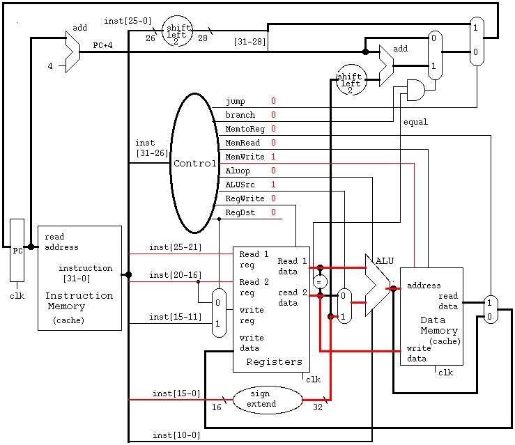 Note the data path around the ALU into the write data input to the memory
The critical control signals are:
jump 0
branch 0
MemRead 0
MemWrite 1
Aluop 0 the ALU performs an add when Aluop is zero
ALUSrc 1
RegWrite 0
The other control signals are shown for completeness.
The add immediate, addi , instruction adds the twos complement
bits 15 downto 0 of the instruction to a register and places the
sum into the destination register. The PC is incremented as shown in
the nop instruction.
The bit pattern for addi in cs411_opcodes.txt
Note the data path around the ALU into the write data input to the memory
The critical control signals are:
jump 0
branch 0
MemRead 0
MemWrite 1
Aluop 0 the ALU performs an add when Aluop is zero
ALUSrc 1
RegWrite 0
The other control signals are shown for completeness.
The add immediate, addi , instruction adds the twos complement
bits 15 downto 0 of the instruction to a register and places the
sum into the destination register. The PC is incremented as shown in
the nop instruction.
The bit pattern for addi in cs411_opcodes.txt
add immediate, addi
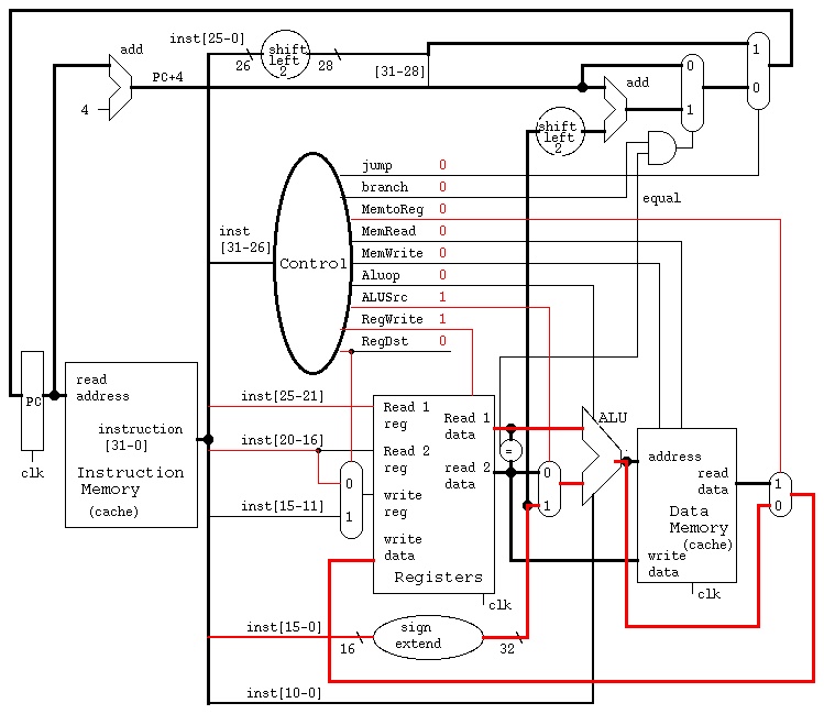 The critical control signals are:
jump 0
branch 0
MemtoReg 0
MemWrite 0
Aluop 0 the ALU performs an add when Aluop is zero
ALUSrc 1
RegWrite 1
RegDst 0
The other control signals are shown for completeness.
The control schematic for some specific instructions, possibly not
this semester, for the one cycle architecture, is:
The critical control signals are:
jump 0
branch 0
MemtoReg 0
MemWrite 0
Aluop 0 the ALU performs an add when Aluop is zero
ALUSrc 1
RegWrite 1
RegDst 0
The other control signals are shown for completeness.
The control schematic for some specific instructions, possibly not
this semester, for the one cycle architecture, is:
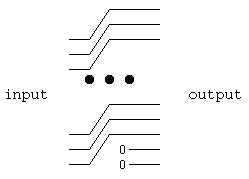
 The shift left 2 circuit is just bent wires.
The VHDL is output <= input(29 downto 0) & "00";
The shift left 2 circuit is just bent wires.
The VHDL is output <= input(29 downto 0) & "00";
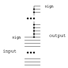
 The sign extend circuit is just wiring. The input is a 16 bit
twos complement word and outputs a 32 bit twos complement word.
The VHDL is output(15 downto 0) <= input;
output(31 downto 16) <= (others => input(15));
The sign extend circuit is just wiring. The input is a 16 bit
twos complement word and outputs a 32 bit twos complement word.
The VHDL is output(15 downto 0) <= input;
output(31 downto 16) <= (others => input(15));
 cs411_opcodes.txt different from Computer Organization and Design 1/8/2020
rd is register destination, the result, general register 1 through 31
rs is the first register, A, source, general register 0 through 31
rt is the second register, B, source, general register 0 through 31
--val---- generally a 16 bit number that gets sign extended
--adr---- a 16 bit address, gets sign extended and added to (rx)
"i" is generally immediate, operand value is in the instruction
Opcode Operands Machine code format
6 5 5 5 5 6 number of bits in field
3 3 2 2 2 2 2 2 2 2 2 2 1 1 1 1 1 1 1 1 1 1
1 0 9 8 7 6 5 4 3 2 1 0 9 8 7 6 5 4 3 2 1 0 9 8 7 6 5 4 3 2 1 0
| | | | |
0 0 0 0 0 0 0 0 0 0 0 0 0 0 0 0 0 0 0 0 0 0 0 0 0 0 0 0 0 0 0 0 nop
0 0 0 0 0 0 a a a a a b b b b b r r r r r -ignored- 1 0 0 0 0 0 add r,a,b
0 0 0 0 0 0 a a a a a b b b b b r r r r r -ignored- 1 0 0 0 1 0 sub r,a,b
0 0 0 0 0 0 a a a a a b b b b b r r r r r -ignored- 0 1 1 0 0 0 mul r,a,b
0 0 0 0 0 0 a a a a a b b b b b r r r r r -ignored- 0 1 1 0 1 1 div r,a,b
0 0 0 0 0 0 a a a a a b b b b b r r r r r -ignored- 0 0 1 1 0 1 and r,a,b
0 0 0 0 0 0 a a a a a b b b b b r r r r r -ignored- 0 0 1 1 1 1 or r,a,b
0 0 0 0 0 0 0 0 0 0 0 b b b b b r r r r r s s s s s 0 0 0 0 1 1 srl r,b,s
0 0 0 0 0 0 0 0 0 0 0 b b b b b r r r r r s s s s s 0 0 0 0 1 0 sll r,b,s
0 0 0 0 0 0 0 0 0 0 0 b b b b b r r r r r -ignored- 0 0 1 0 1 1 cmpl r,b
0 0 0 0 1 0 -----address to bits (27:2) of PC------------------ j adr
0 0 1 1 1 1 x x x x x r r r r r ---2's complement value-------- lwim r,val(x)
0 0 1 1 0 0 x x x x x r r r r r ---2's complement value-------- addi r,val(x)
0 1 1 1 0 1 a a a a a b b b b b ---2's complement address------ beq a,b,adr
1 0 0 0 1 1 x x x x x r r r r r ---2's complement address------ lw r,adr(x)
1 0 1 0 1 1 x x x x x b b b b b ---2's complement address------ sw b,adr(x)
Definitions:
nop no operation, no programmer visible registers or memory
are changed, except PC <= PC+4
j adr bits 0 through 25 of the instruction are inserted into PC(27:2)
probably should zero bits PC(1:0) but should be zero already
lw r,adr(x) load word into register r from memory location (register x plus
sign extended adr field)
sw b,adr(x) store word from register b into memory location (register x plus
sign extended adr field)
beq a,b,adr branch on equal, if the contents of register a are equal
to the contents of register b, add the, shifted by two,
sign extended adr to the PC (The PC will have 4 added by then)
lwim r,val(x) add immediate, the contents of register x is added to the
sign extended value and the result put into register r
addi r,val(x) add immediate, the contents of register x is added to the
sign extended value and the result is added to register r
add r,a,b add register a to register b and put result into register r
sub r,a,b subtract register b from register a and put result into register r
mul r,a,b multiply register a by register b and put result into register r
div r,a,b divide register a by register b and put result into register r
and r,a,b and register a to register b and put result into register r
or r,a,b or register a to register b and put result into register r
srl r,b,s shift the contents of register b by s places right and put
result in register r
sll r,b,s shift the contents of register b by s places left and put
result in register r
cmpl r,b one's complement of register b goes into register r
Also: no instructions are to have side effects or additional "features"
last updated 1/8/2020 (slight difference in opcodes from previous semesters)
cs411_opcodes.txt different from Computer Organization and Design 1/8/2020
rd is register destination, the result, general register 1 through 31
rs is the first register, A, source, general register 0 through 31
rt is the second register, B, source, general register 0 through 31
--val---- generally a 16 bit number that gets sign extended
--adr---- a 16 bit address, gets sign extended and added to (rx)
"i" is generally immediate, operand value is in the instruction
Opcode Operands Machine code format
6 5 5 5 5 6 number of bits in field
3 3 2 2 2 2 2 2 2 2 2 2 1 1 1 1 1 1 1 1 1 1
1 0 9 8 7 6 5 4 3 2 1 0 9 8 7 6 5 4 3 2 1 0 9 8 7 6 5 4 3 2 1 0
| | | | |
0 0 0 0 0 0 0 0 0 0 0 0 0 0 0 0 0 0 0 0 0 0 0 0 0 0 0 0 0 0 0 0 nop
0 0 0 0 0 0 a a a a a b b b b b r r r r r -ignored- 1 0 0 0 0 0 add r,a,b
0 0 0 0 0 0 a a a a a b b b b b r r r r r -ignored- 1 0 0 0 1 0 sub r,a,b
0 0 0 0 0 0 a a a a a b b b b b r r r r r -ignored- 0 1 1 0 0 0 mul r,a,b
0 0 0 0 0 0 a a a a a b b b b b r r r r r -ignored- 0 1 1 0 1 1 div r,a,b
0 0 0 0 0 0 a a a a a b b b b b r r r r r -ignored- 0 0 1 1 0 1 and r,a,b
0 0 0 0 0 0 a a a a a b b b b b r r r r r -ignored- 0 0 1 1 1 1 or r,a,b
0 0 0 0 0 0 0 0 0 0 0 b b b b b r r r r r s s s s s 0 0 0 0 1 1 srl r,b,s
0 0 0 0 0 0 0 0 0 0 0 b b b b b r r r r r s s s s s 0 0 0 0 1 0 sll r,b,s
0 0 0 0 0 0 0 0 0 0 0 b b b b b r r r r r -ignored- 0 0 1 0 1 1 cmpl r,b
0 0 0 0 1 0 -----address to bits (27:2) of PC------------------ j adr
0 0 1 1 1 1 x x x x x r r r r r ---2's complement value-------- lwim r,val(x)
0 0 1 1 0 0 x x x x x r r r r r ---2's complement value-------- addi r,val(x)
0 1 1 1 0 1 a a a a a b b b b b ---2's complement address------ beq a,b,adr
1 0 0 0 1 1 x x x x x r r r r r ---2's complement address------ lw r,adr(x)
1 0 1 0 1 1 x x x x x b b b b b ---2's complement address------ sw b,adr(x)
Definitions:
nop no operation, no programmer visible registers or memory
are changed, except PC <= PC+4
j adr bits 0 through 25 of the instruction are inserted into PC(27:2)
probably should zero bits PC(1:0) but should be zero already
lw r,adr(x) load word into register r from memory location (register x plus
sign extended adr field)
sw b,adr(x) store word from register b into memory location (register x plus
sign extended adr field)
beq a,b,adr branch on equal, if the contents of register a are equal
to the contents of register b, add the, shifted by two,
sign extended adr to the PC (The PC will have 4 added by then)
lwim r,val(x) add immediate, the contents of register x is added to the
sign extended value and the result put into register r
addi r,val(x) add immediate, the contents of register x is added to the
sign extended value and the result is added to register r
add r,a,b add register a to register b and put result into register r
sub r,a,b subtract register b from register a and put result into register r
mul r,a,b multiply register a by register b and put result into register r
div r,a,b divide register a by register b and put result into register r
and r,a,b and register a to register b and put result into register r
or r,a,b or register a to register b and put result into register r
srl r,b,s shift the contents of register b by s places right and put
result in register r
sll r,b,s shift the contents of register b by s places left and put
result in register r
cmpl r,b one's complement of register b goes into register r
Also: no instructions are to have side effects or additional "features"
last updated 1/8/2020 (slight difference in opcodes from previous semesters)
<- previous index next ->