<- previous index next ->
Personal effort plus automation:
Your plane will be ready soon
Basic decimal addition (with carry digit shown)
101 <- carry (note that three numbers are added after first digit)
567
+ 526
-----
1093
Binary addition (with carry bit shown)
1011 <- carry (note that three bits are added after first bit)
for future reference c(3)=1, c(2)=0, c(1)=1, c(0)=1
1011 bits are numbered from zero, right to left
+ 1001
-----
10100 for future reference s(3)=0, s(2)=1, s(1)=0, s(0)=0
the leftmost '1' is cout
Since three bits must be added, a truth table for a full adder
needs three inputs and thus eight entries.
a b c | s co
------+----- _ _ _ _ _ _
0 0 0 | 0 0 s = (a*b*c) + (a*b*c) + (a*b*c) + (a*b*c)
0 0 1 | 1 0 simplifies to
0 1 0 | 1 0 s = a xor b xor c
0 1 1 | 0 1 s <= a xor b xor c;
1 0 0 | 1 0 _ _ _
1 0 1 | 0 1 co = (a*b*c) + (a*b*c) + (a*b*c) + (a*b*c)
1 1 0 | 0 1 simplifies to
1 1 1 | 1 1 co = (a*b)+(a*c)+(b*c)
co <= (a and b) or (a and c) or (b and c);
This can be drawn as a box for use on larger schematics
+-------+
| a b c | The inputs are shown at the top (or right)
| |
| fadd |
| |
| co s | The outputs are shown at the bottom (or left)
+-------+
This is easier than copying as a schematic
The full adder can be written as an entity in VHDL
entity fadd is -- full stage adder, interface
port(a : in std_logic;
b : in std_logic;
c : in std_logic;
s : out std_logic;
co : out std_logic);
end entity fadd;
architecture circuits of fadd is -- full adder stage, body
begin -- circuits of fadd
s <= a xor b xor c after 1 ns;
co <= (a and b) or (a and c) or (b and c) after 1 ns;
end architecture circuits; -- of fadd
The full adder can be written as a module in Verilog
module fadd(a, b, cin, sum, cout); // from truth table
input a; // a input
input b; // b input
input cin; // carry-in
output sum; // sum output
output cout; // carry-out
assign sum = (~a*~b*cin)+(~a*b*~cin)+(a*~b*~cin)+(a*b*cin);
assign cout = (a*b)+(a*cin)+(b*cin); // last term redundant
endmodule // fadd
Connecting four full adders, four fadd's, to make a 4-bit adder
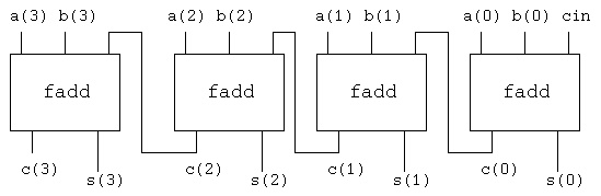 c(3) should be cout
The connections are written for VHDL as
a0: entity WORK.fadd port map(a(0), b(0), cin, s(0), c(0));
a1: entity WORK.fadd port map(a(1), b(1), c(0), s(1), c(1));
a2: entity WORK.fadd port map(a(2), b(2), c(1), s(2), c(2));
a3: entity WORK.fadd port map(a(3), b(3), c(2), s(3), cout);
The connections are written for Verilog as
// instantiate modules
fadd bit0(a[0], b[0], cin, sum[0], c[0]);
fadd bit1(a[1], b[1], c[0], sum[1], c[1]);
fadd bit2(a[2], b[2], c[1], sum[2], c[2]);
fadd bit3(a[3], b[3], c[2], sum[3], cout);
Note that the carry out of the previous stage is wired into
the carry input of the next higher stage. In a computer,
four bits are added to four bits and this produces four bits of sum.
The last carry bit, c(3) here, is usually called 'cout' and is
not called a 'sum' bit.
The VHDL circuit was simulated with
a(3)=0, a(2)=0, a(1)=0, a(0)=1 cin=0
b(3)=1, b(2)=1, b(1)=1, b(0)=1
There is a small delay time from the input to the output.
When a circuit is simulated, the initial values of signals
are shown as 'U' for uninitialized. As the circuit simulation
proceeds, the 'U' are computed and become '0' or '1'.
Partial output from the VHDL simulation shows this propagation.
(the upper line is logic '1', the lower line is logic '0')
s(0) UU_____________________________
s(1) UUUUUU_________________________
s(2) UUUUUUUUUU_____________________
s(3) UUUUUUUUUUUUUU_________________
____________________________
c(0) UU
________________________
c(1) UUUUUU
____________________
c(2) UUUUUUUUUU
________________
c(3) UUUUUUUUUUUUUU
At the end of the simulation the values are:
s(0)=0, s(1)=0, s(2)=0, s(3)=0, c(0)=1, c(1)=1, c(2)=1, c(3)=1
The full VHDL code is add_trace.vhdl
The run file is add_trace.run
The full output file is add_trace.out
A fragment of the Makefile is Makefile.add_trace
The Verilog code is
add4.v
add4_v.out
The Verilog output ran three cases:
add4.v running
a=1011, b=1000, cin=1, sum=0100, cout=1
a=0000, b=0000, cin=0, sum=0000, cout=0
a=1111, b=1111, cin=1, sum=1111, cout=1
L52 "add4.v": $finish at simulation time 15
Subtract
Given that the computer can "add" it now has to be able to "subtract."
Thus, a representation has to be chosen for negative numbers.
All computers have chosen the left most bit (also called the
high-order bit) to be the sign bit. The convention is that a '1'
in the sign bit means negative, a '0' in the sign bit means positive.
Within these conventions, three representations have been used
in computers: two's complement, one's complement and sign magnitude.
All bits are shown for 4-bit words in the table below.
decimal twos complement ones complement sign magnitude
0 0000 0000 0000
1 0001 0001 0001
2 0010 0010 0010
3 0011 0011 0011
4 0100 0100 0100
5 0101 0101 0101
6 0110 0110 0110
7 0111 0111 0111
-8 1000 - -
-7 1001 1000 1111
-6 1010 1001 1110
-5 1011 1010 1101
-4 1100 1011 1100
-3 1101 1100 1011
-2 1110 1101 1010
-1 1111 1110 1001
-0 - 1111 1000
We could choose to build a subtractor that uses a borrow, yet
this would require as many gates as were needed for the adder.
By choosing the two's complement representation of negative
numbers, an adder with a relatively low gate count multiplexor
and inverter can become a subtractor. The implementation follows
the definition of a negative number in two's complement
representation: invert the bits and add one.
Given a new symbol for an adder, the complete circuit for
doing 4-bit add and subtract becomes:
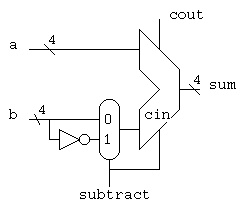 When the signal "subtract" is '1' the circuit subtracts 'b' from 'a'.
When the signal "subtract" is '0' the circuit adds 'a' to 'b'.
The basic circuit is written for VHDL as:
a4: entity work.add4 port map(a, b_mux, subtract, sum, cout);
i4: b_bar <= not b;
m4: entity work.mux4 port map(b, b_bar, subtract, b_mux);
The general rule is that each circuit component symbol on
a schematic diagram will become one VHDL statement.
There are many other VHDL statements needed to run a complete
simulation.
The annotated output of the simulation is:
subtract=0, a=0100, b=0010, sum=0110 4+2=6
subtract=1, a=0100, b=0010, sum=0010 4-2=2
subtract=0, a=1100, b=0010, sum=1110 (-4)+2=(-2)
subtract=1, a=1100, b=0010, sum=1010 (-4)-2=(-6)
subtract=0, a=1100, b=1110, sum=1010 (-4)+(-2)=(-6)
subtract=1, a=1100, b=1110, sum=1110 (-4)-(-2)=(-2)
subtract=0, a=0011, b=1110, sum=0001, 3+(-2)=1
subtract=1, a=0011, b=1110, sum=0101, 3-(-2)=5
The full VHDL code is sub4.vhdl
The run file is sub4.run
The full output file is sub4.out
A fragment of the Makefile is Makefile.sub4
Somewhat similar Verilog code, using 4 bit mux
sub4.v
sub4_v.out
Checking both add and subtract:
sub4.v running
add
a=1011, b=1000, cin=1, sum=0100, cout=1
in0=1000, in1=0111, ctl=0, b=1000
subtract
a=1011, b=0111, cin=1, sum=0011, cout=1
in0=1000, in1=0111, ctl=1, b=0111
add
a=0000, b=0000, cin=0, sum=0000, cout=0
in0=0000, in1=1111, ctl=0, b=0000
subtract
a=0000, b=1111, cin=0, sum=1111, cout=0
in0=0000, in1=1111, ctl=1, b=1111
add
a=1111, b=1111, cin=1, sum=1111, cout=1
in0=1111, in1=0000, ctl=0, b=1111
subtract
a=1111, b=0000, cin=1, sum=0000, cout=1
in0=1111, in1=0000, ctl=1, b=0000
L113 "sub4.v": $finish at simulation time 30
When the signal "subtract" is '1' the circuit subtracts 'b' from 'a'.
When the signal "subtract" is '0' the circuit adds 'a' to 'b'.
The basic circuit is written for VHDL as:
a4: entity work.add4 port map(a, b_mux, subtract, sum, cout);
i4: b_bar <= not b;
m4: entity work.mux4 port map(b, b_bar, subtract, b_mux);
The general rule is that each circuit component symbol on
a schematic diagram will become one VHDL statement.
There are many other VHDL statements needed to run a complete
simulation.
The annotated output of the simulation is:
subtract=0, a=0100, b=0010, sum=0110 4+2=6
subtract=1, a=0100, b=0010, sum=0010 4-2=2
subtract=0, a=1100, b=0010, sum=1110 (-4)+2=(-2)
subtract=1, a=1100, b=0010, sum=1010 (-4)-2=(-6)
subtract=0, a=1100, b=1110, sum=1010 (-4)+(-2)=(-6)
subtract=1, a=1100, b=1110, sum=1110 (-4)-(-2)=(-2)
subtract=0, a=0011, b=1110, sum=0001, 3+(-2)=1
subtract=1, a=0011, b=1110, sum=0101, 3-(-2)=5
The full VHDL code is sub4.vhdl
The run file is sub4.run
The full output file is sub4.out
A fragment of the Makefile is Makefile.sub4
Somewhat similar Verilog code, using 4 bit mux
sub4.v
sub4_v.out
Checking both add and subtract:
sub4.v running
add
a=1011, b=1000, cin=1, sum=0100, cout=1
in0=1000, in1=0111, ctl=0, b=1000
subtract
a=1011, b=0111, cin=1, sum=0011, cout=1
in0=1000, in1=0111, ctl=1, b=0111
add
a=0000, b=0000, cin=0, sum=0000, cout=0
in0=0000, in1=1111, ctl=0, b=0000
subtract
a=0000, b=1111, cin=0, sum=1111, cout=0
in0=0000, in1=1111, ctl=1, b=1111
add
a=1111, b=1111, cin=1, sum=1111, cout=1
in0=1111, in1=0000, ctl=0, b=1111
subtract
a=1111, b=0000, cin=1, sum=0000, cout=1
in0=1111, in1=0000, ctl=1, b=0000
L113 "sub4.v": $finish at simulation time 30
<- previous index next ->
Other links
Go to top