<- previous index next ->
Several views of computers to follow:
rip->instruction->decode->registers->alu->ear->data RAM etc.
First, a very complex computer architecture, the Itanium, IA_64
Just look at all those registers!
Then at end, three level cache.
cs411_IA_64.pdf
Probably need to do firefox cs411_IA_64.pdf
or use Adobe Reader /afs/umbc.edu/users/s/q/squire/pub/www/images/cs411_IA_64.pdf
Block diagram of typical Intel computer.
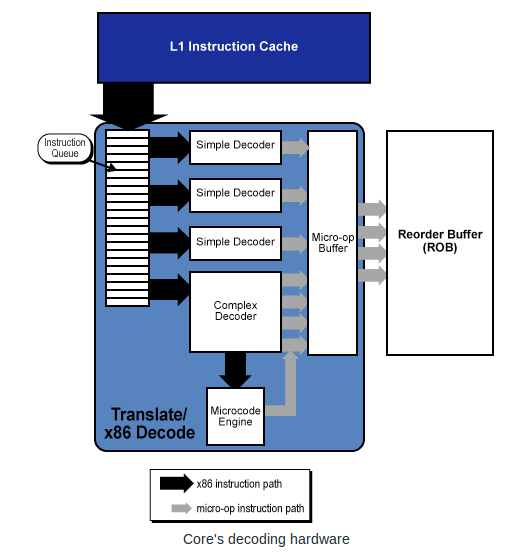
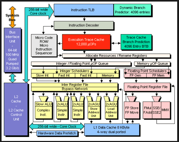 Modern Intel computers do not directly execute our assembly language
instructions. Decoders are used to make a sequence of RISC instructions,
executed in the "simple architecture" below.
Hyper Threading, just another "Hyper"
Before and after Hyper
Very small addition increased average execution from
2.5 instructions per clock to 3.5 instructions per clock
on some applications.
Modern Intel computers do not directly execute our assembly language
instructions. Decoders are used to make a sequence of RISC instructions,
executed in the "simple architecture" below.
Hyper Threading, just another "Hyper"
Before and after Hyper
Very small addition increased average execution from
2.5 instructions per clock to 3.5 instructions per clock
on some applications.
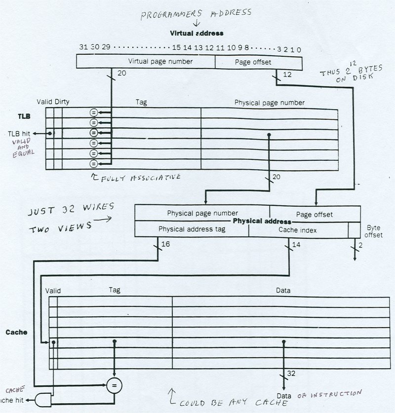
 The computer architecture has a TLB, translation lookaside buffer
that translates the addresses you see in the debugger, "virtual addresses"
into a "physical address" actual RAM addresses.
That address then goes into a cache that may have the RAM data or
instruction, thus avoiding the slow RAM access.
One TLB with cache looks like the figure below.
The computer architecture has a TLB, translation lookaside buffer
that translates the addresses you see in the debugger, "virtual addresses"
into a "physical address" actual RAM addresses.
That address then goes into a cache that may have the RAM data or
instruction, thus avoiding the slow RAM access.
One TLB with cache looks like the figure below.
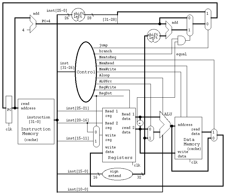
 Now, a very simple architecture to follow and instruction execution.
This is after decoding instructions and TLB and cache.
PC program counter is the rip instruction pointer as a RAM address.
Instruction Memory would be section .text
Data Memory would be section .data and section .bss
ALU executes instructions mov, add, sub, imul, idiv, shift, etc.
This architecture is not Intel.
This is 32 bit MIPS computer used in SGI computers (We had one here at UMBC).
Now, a very simple architecture to follow and instruction execution.
This is after decoding instructions and TLB and cache.
PC program counter is the rip instruction pointer as a RAM address.
Instruction Memory would be section .text
Data Memory would be section .data and section .bss
ALU executes instructions mov, add, sub, imul, idiv, shift, etc.
This architecture is not Intel.
This is 32 bit MIPS computer used in SGI computers (We had one here at UMBC).
 CS411 opcodes, instruction formats
mips opcodes, instruction formats
CS411 opcodes, instruction formats
mips opcodes, instruction formats
<- previous index next ->