The DLX Processor

For this class, you'll be designing a processor that implements a subset of the DLX instruction set. This subset was chosen to keep the project simple, allowing undergraduates complete the design in a single semester. Nevertheless, this processor has most of the ingredients of a "real" CPU. By the end of the semester, you'll be able to run simple programs on the processor, allowing you to observe the internal operations of a CPU as it executes instructions. This project may seem large at first; that's because you're getting the entire description all at the start of the semester. There will be checkpoints throughout the semester, giving you opportunities to make sure you're on the right track. As you'll see, this project can be broken down into several smaller parts, each of which is small enough to complete in a few weeks.

Overview

The DLX processor uses a load-store architecture similar to that of the MIPS processor we'll be discussing in class. As with the MIPS processor, all DLX instructions are 32 bits long. This decision makes the design considerably easier - fetching an instruction is merely a matter of reading the next 4-byte word from memory.

The DLX processor has 32 registers, each of which is 32 bits long. However, two of these registers are reserved for special purposes. Register 0 always contains zero. It can be used as a source operand whenever zero is needed, and stores to it have no effect. Register 31 is reserved for use by some DLX instructions, as will be described shortly. DLX also has a 32 bit program counter.

Instruction Set

Instruction Formats

There are three instruction formats in DLX: R-type, I-type, and J-type. All instruction formats must specify an opcode; however, the other information in the instruction varies by format. R-type (register) instructions specify three registers in the instruction - two source registers and one destination register. I-type (immediate) instructions specify one source register, one destination register, and a 16-bit immediate value that is sign-extended to 32 bits before it's used. J-type (jump) instructions consist of just the opcode and a 26 bit operand, which is used to calculate the destination address.

These three instruction formats are summarized in this table:

FormatBits
 31        26 25          21 20          16 15          11 10          6 5          0
R-type0x0Rs1 Rs2Rd unused opcode
I-typeopcodeRs1 Rd immediate
J-typeopcode value

Instructions

This table lists the instructions that your implementation of DLX must support. The ``real'' DLX includes additional instructions, including some to support floating point calculations. These were left out to simplify implementation. NOTE: the operations for each opcode are specified using C syntax and operators. All immediate values are padded with zeros on the left unless indicated by extend(), in which case they are padded with copies of the left-most bit in the immediate value. Also, some instructions don't use all of the fields available for the format.

Instr. Description Format Opcode Operation (C-style coding)
ADD add R 0x20 Rd = Rs1 + Rs2
ADDI add immediate I 0x08 Rd = Rs1 + extend(immediate)
AND and R 0x24 Rd = Rs1 & Rs2
ANDI and immediate I 0x0c Rd = Rs1 & immediate
BEQZ branch if equal to zero I 0x04 PC += (Rs1 == 0 ? extend(immediate) : 0)
BNEZ branch if not equal to zero I 0x05 PC += (Rs1 != 0 ? extend(immediate) : 0)
J jump J 0x02 PC += extend(value)
JAL jump and link J 0x03 R31 = PC + 4 ; PC += extend(value)
JALR jump and link register I 0x13 R31 = PC + 4 ; PC = Rs1
JR jump register I 0x12 PC = Rs1
LHI load high bits I 0x0f Rd = immediate << 16
LW load woRd I 0x23 Rd = MEM[Rs1 + extend(immediate)]
OR or R 0x25 Rd = Rs1 | Rs2
ORI or immediate I 0x0d Rd = Rs1 | immediate
SEQ set if equal R 0x28 Rd = (Rs1 == Rs2 ? 1 : 0)
SEQI set if equal to immediate I 0x18 Rd = (Rs1 == extend(immediate) ? 1 : 0)
SLE set if less than or equal R 0x2c Rd = (Rs1 <= Rs2 ? 1 : 0)
SLEI set if less than or equal to immediate I 0x1c Rd = (Rs1 <= extend(immediate) ? 1 : 0)
SLL shift left logical R 0x04 Rd = Rs1 << (Rs2 % 8)
SLLI shift left logical immediate I 0x14 Rd = Rs1 << (immediate % 8)
SLT set if less than R 0x2a Rd = (Rs1 < Rs2 ? 1 : 0)
SLTI set if less than immediate I 0x1a Rd = (Rs1 < extend(immediate) ? 1 : 0)
SNE set if not equal R 0x29 Rd = (Rs1 != Rs2 ? 1 : 0)
SNEI set if not equal to immediate I 0x19 Rd = (Rs1 != extend(immediate) ? 1 : 0)
SRA shift right arithmetic R 0x07 as SRL & see below
SRAI shift right arithmetic immediate I 0x17 as SRLI & see below
SRL shift right logical R 0x06 Rd = Rs1 >> (Rs2 % 8)
SRLI shift right logical immediate I 0x16 Rd = Rs1 >> (immediate % 8)
SUB subtract R 0x22 Rd = Rs1 - Rs2
SUBI subtract immediate I 0x0a Rd = Rs1 - extend(immediate)
SW store woRd I 0x2b MEM[Rs1 + extend(immediate)] = Rd
XOR exclusive or R 0x26 Rd = Rs1 ^ Rs2
XORI exclusive or immediate I 0x0e Rd = Rs1 ^ immediate

There are a few additional notes on the instructions.

External Signals

As with any processor, the DLX CPU needs to talk to the outside world. It can do this via a few simple signals. In addition to a data and address bus (with the necessary control signals), DLX needs a RESET signal and a clock. These signals and buses are described in this section.

RESET Signal

As with all processors, there must be some way of getting the CPU into a known state. This must be done after the CPU is "powered up", and can be done at other times to restore the CPU to a reasonable starting point. DLX uses the RESET signal for this purpose. When the RESET signal is asserted (high), the CPU loads the program counter with 0. After RESET is deasserted, execution begins at location 0, which should probably be the address of the first instruction of a program to be executed.

Clock

The DLX processor, like just about every other processor, requires an external clock signal. This can be provided in one of two ways. For debugging, a "manual" clock signal is likely to be the best. This signal should allow the user to manually set the clock signal to high and low alternately. Since this CPU is being designed in a simulator and cycle time is unimportant, this method will allow you to take your time examining the CPU after each clock cycle.

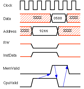
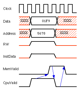
Once your CPU is working, however, you may want to use a "real" clock. If so, you can create one in the simulator. However, make sure your cycle time is sufficiently long. If it isn't, your CPU may not work.

Memory Interface

A CPU is only as good as the program and data it uses. The memory interface is the only way to get data in and out of the DLX CPU, so it's important that it work properly. However, real processor designs often introduce lots of complexity to insure peak performance. In this class, however, performance is somewhat sacrificed for ease of design, reducing the number of control lines necessary for the memory interface.

The signals in the memory interface are:

The Address and Data signals are self-explanatory - they contain the address of the memory access and the data for the access. For a write, the data is driven by the CPU. For a read, the memory drives the data. InstData is driven by the CPU to 0 if the access is an instruction fetch, and 1 if the access is for data (read or write). RW is driven by the CPU to indicate whether the access is a memory read (RW = 0) or write (RW = 1). CpuValid is set by the CPU to indicate when the signals on Address, InstData, RW, and Data (for writes) are valid. MemValid is used by the memory to indicate when Data contains valid signals being driven by memory (for a read). The following diagrams show a sample read and write bus transaction. Note that all lines may only be sampled on the rising edge of the clock signal unless the signal is required to stay constant until the next rising edge (ie, a memory address in the middle of a memory read transaction).

Sample Timing Diagrams

Signals whose value is indeterminate are shown in red. The arrows in blue indicate the ordering for changes in the MemValid and CpuValid signals.

A sample memory data read transaction (reading the value 0x588 from the location 0x9244) is shown to the right. The same sequence would be followed for an instruction read, except that InstData would be set to 0 rather than 1.

To start the transaction, the CPU asserts Address, RW, and InstData. These must be stable every time CpuValid is 1 on a rising clock edge. They must stay at the same value until CpuValid is set to 0. This happens only after MemValid is set to 1 and Data is read on the rising edge. Note that Data can be read on the first rising edge for which MemValid is 1. To end the transaction, MemValid is set to 0; this can't occur until after memory has seen CpuValid set to 0 on a rising edge. At this point, another memory transaction may start.

Sample memory read transaction
A sample memory data write transaction (writing the value 0x1f9 to the location 0x5678) is shown to the right. Note that InstData should always be 1 for a write, since instructions are never written to memory. Sample memory write transaction


[Back] Go back to the main page.
Last updated 9 Feb 1996 by Ethan Miller (elm@cs.umbc.edu)